50W
MONOBLOC PP CLASS AB SS AMP.
Updated 2018.
This page about 2 x 50W class A amps with mosfets and OPT.
Content:-
Picture 1. 2 x 50W monobloc class A amps.
Fig 1. Schematic 50W amp + PSU, 3 x small bjts and 4 x 2SK134,
OPT, fixed bias.
Schematic explained.
Graph 1. 2SK134 Eds Vs Ids characteristics with load lines.
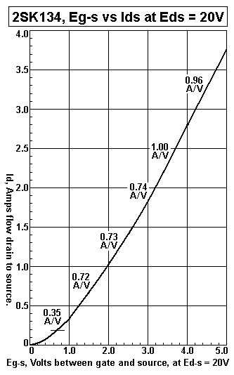
Graph 2. 2SK134 Id vs Egs character and gm shown.
2SK134 design parameters of µ, Rd and gm. Mosfet gain
calculations,
3 loops of NFB explained.
Picture 2. Inside of 50W monobloc.
Fig 2. Schematic of Basic Model of SE mosfet amp with 1 x bjt and
1 x 2SK134
output mosfet with all voltage + current path calculations, more
on NFB.
Shunt NFB explained, alternative B+, loads, power, psu notes,
heatsinks.
Notes on SE mosfet designs with choke feed and cap coupling,
class A PP alternatives. Picture of inside the amp.
Fig 3. 50W OPT details for 50W monoblocs.
About partial air gapping, core types.
2SK134 properties, gm, Rd, µ.
About heatsinks for class A.
Fig 4. Schematic of 2 x EL84 used to drive 4 x 2SK134 or 2SK1058.
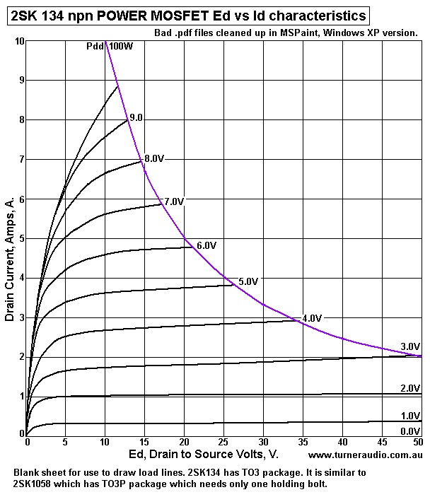
Fig 7. 2SK134 Blank sheet for drawing load
lines.......
Picture 1. 2 x 50W mono amps on bench.
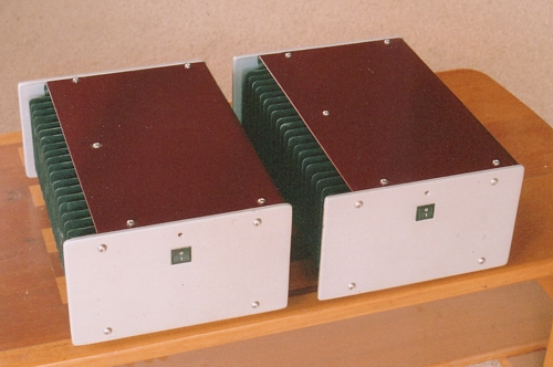
In 2000 I built the above pair of 50W class A SS amps using 4 x
Hitachi 2SK134 per channel,
and I used a similar amp topology to use of 2 small input pentodes
and 4 output EL34 pentodes in
a normal PP amp.
The input and driver stage uses three generic TO92 package npn
bjts for a differential pair
( Long Tail Pair ) with a CCS common emitter current sink. The
collectors of LTP are capacitance
coupled to gates of 4 npn mosfets with a fixed +Vdc bias applied.
Output mosfets drive a wide
bandwidth OPT. The use of only npn mosfets in a PP output stage
gives very low distortion compared
to use of pnp + npn mosfets which are not naturally well matched
for their biasing or transfer function.
Use of an OPT prevents any speaker from ever being directly
connected to a Vdc rail if an mosfet fails
by becoming a short circuit, which they do when someone uses a
shorted speaker cable for a few minutes
on low power without realizing anything is wrong. I had the spare
time and the spare materials laying
around, so I developed the following schematic:-
Fig 1. PP 50W mosfet amp.
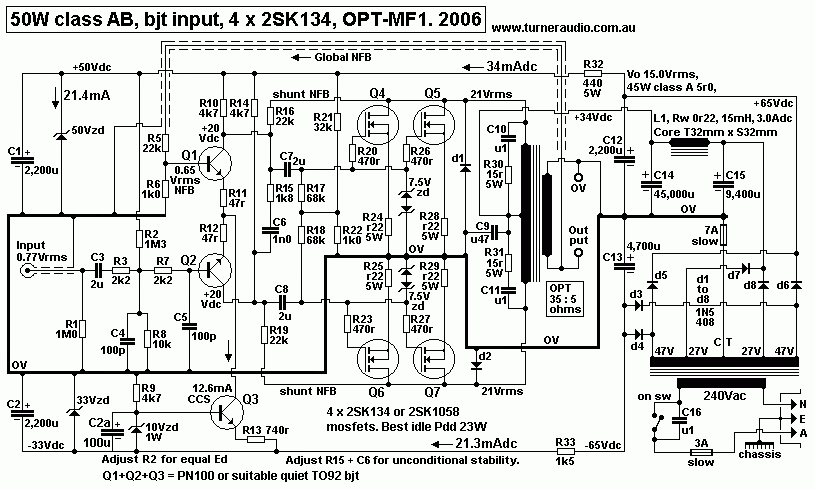
Input Q1 and Q2 are BC546 but may be many other type, PN100 are
OK, and these form an
input differential amp aka long tail pair aka LTP with 2 x Q3
BC546 as the pair, and BC109 as
a low noise constant current sink aka CCS to sink the 2 x 6.3mAdc
Idc Q1+2 from commoned
emitters.
Q1 and Q2 have medium voltage gain due to 47r R11+R12 for local
current FB and they are
quite linear while handling max Ic signal current of +/-1.8mApk,
and producing less than +/- 2Vpk
at each collector during most normal operation without
clipping.
Input to power amp Q2 has 2uF feeding network including R8 10k for
-3dB LF pole = 6.6Hz
The preamp may have a similar pole, giving -6dB at 6.6 and maybe
-3dB at about 10Hz = OK.
The input signal is to Q2 base with GNFB to Q1 base.
The output stage Q4-Q7 are four 2SK134 N type Hitachi output
mosfets with idle Ed = +33Vdc
and idle current 0.7Adc each for Pdd = 23.1W. Total Pdd = 92.4W,
and maximum class A possible
at 46% efficiency = 43W max at mosfet drain output.
3W is lost as heat in Rw in OPT so max class A Po = 40W at OPT
secondary terminals.
The B+ supply is nominally +35Vdc at C15, which drops slightly to
+34Vdc at OPT CT because of
L1 choke resistance.
The 2SK134 are from 1980s and considered excessively ancient, and
not available except as NOS.
There may be better types now in 2016, but from what I have seen
and read, most modern types
are just not made with the same benign negative temperature
co-efficient for the idle current I want
to use to maximize class A operation. The modern types have far
higher specs for max currents and
very high gm, but when you examine most power mosfets you will
find gm not much better than
2SK134 at the idle Idc for class A. Gm tends to vary hugely with
the current for more modern mosfets.
2SK1058 is a very suitable TO3P package that is is slightly less
ancient but is very good for this use.
While in class A, the Id varies between idle at +0.7A up to +1.4A
pk max and down to 0.0A.
But inevitably, someone will try to use use a 2r5r load instead of
5r0 and the OPT Pri RLd-d load
becomes 17r0, so that mosfets have cut off for part of wave cycle
and the pair on each side have max
load = 4.3r, and if Vd = 21Vrms, peak Id in each mosfet is 3.5Apk,
and if average gm = 0.9A/V
the Vgs is about 4V, and there is 0.8V across 0.22r so max Vg-0V
needed is about 4.8Vpk.
I measured 2SK134 to have :-
Amplification factor, µ = 180 to 200, Dynamic drain resistance, Rd
= 257r to 220r approx,
Transconductance, Gm = 0.7 to 0.9 Amps / Volt, for Id = 0.7A to
2A.
The µ, Rd, and Gm vary considerably between Id min = 0.0A and Id
max = 2Apk.
The region of interest is the low power operation where Id varies
less than +/- 10% around the idle Iadc.
2SK134 has very high gate input resistance like a tube but Cg-s =
600pF. Cg-d = 11pF which can
to about 210pF if gain = 19 for high class A RLd.
Note. There is more variation to Gm and Rd than I measured.....
As the Sec loads are reduced, so to are the drain loads, and
nominally 6r0 speakers can vary between 4r0
and 40r0, the the output Vo is held constant by NFB loops if input
is kept constant so that the F response of
Vg-s varies with load changes at different frequencies. This
occurs in all analog amps with loop NFB.
But the Vg-0V and hence Vg-s is limited to +/-8Vpk by back to back
7.5V zener diodes. Thus max Id is
limited to about 6Apk.
Data for 2SK134 shows they have 12V zener diodes back to back
within the case as well as a diode from d to s
to prevent flow of Idc that is opposite to normal direction shown.
Consider Sec output load = 1r0.
OPT TR = 2.58 : 1. For 1/2 Pri to Sec it is 1.29 : 1, and ZR =
1.66 :1. For 1r0 at Sec, RLd at Pri = 1.66r
plus total RwP + RwS = 0.95r = 2.61r. This is OPT load for 2
mosfets.
Therefore EACH mosfet on each side of PP circuit has Pri load
of 2 x 2.61r = 5.22r and you must add 0.22r
= 5.44r. Loadline analysis tells me Ipk = 5.3Apk, and Vg = +8Vpk
and there will be about +1.17Vpk
at Rs 0.22r so Vg-0V = +9.17Vpk, but you could not have the 7.5V
zener diodes because they will limit
Vg-0V to +8Vpk.
Graph 1. Loadlines for pure class A and class AB, for 1 x
2SK134.
Graph 2. Id Vs Eg curve at 20V showing mild variation of Gm
from 0.15A to 4A.
Graph 1 shows loadlines RLd for one 2SK134 within one PP pair
working, with RLd including total RwP+S + Rs
so that any Po calculated from possible Vd and Id swings includes
wasted Po in RwP+S + Rs.
For 1r0 load at Sec of OPT-MF1, max Id is 5.4A For B RLd = 5.44r
but to get that the Vgs must be +9Vpk.
The PP load for the PP pair = 21.76, and you can see the Rd curves
become crowded above Id 4.5Apk and
you would find HD without any NFB may be 8%, nearly all 3H but at
1/2 Po, maybe only 2% and 20dB NFB
would much reduce the HD.
Graph 2 shows the gm at ONE Ed = 20V, and the curve for Id vs Egs
assumed load = 0.0r, ie, the vertical
line at Ed = 20V. And the gm only varies from 0.72A/V to 0.96A/V
for 3.5A change of Id.
In Graph 1, the shape of the knee of Rd curves is more rounded as
Id increases so that Gm reduces as Id
increased and Ed reduces.
But the linearity is quite good compared to many other
devices, so the Japanese Mosfet Masters really knew
what they were doing IMHO.
For high RLd values and pure class A PP action for line AQB the
higher gain means amount of NFB is higher
and you could expect THD > 0.5% at 21W from the PP pair.
For 4 mosfets with 1r0 at OPT sec, nominal RLd-d = 10.9r, and you
can see that Ed minimum = 3.5Vpk
and for Eds = 33Vdc, Vds swing is 29.5Vpk = 20.85Vrms and Vd-d =
41.7Vrms and max drain Po
= 159.6W.
But loss in RwP+S and Rs = 100% x series R / ( Series R + ZR x Sec
RL )
= 100% x 1.06r / ( 1.06r + 1.66r ) = 39%.
So the power at Sec RL 1r0 = 159.6 -39% = 97.3W.
But in fact the theoretical max continuous Po would be less
because B+ rail sag from +34V to maybe
+30V, reducing Vd-d to 36.0Vrms giving 118W at drains and
72W at OPT Sec.
I show the 7.5V back to back zener diodes which limit Vg-0V to +/-
8Vpk. The bias Vg=0V is about
+1.6Vdc so max Po to 1.0 would be much less than 72W, possibly
only 40W.
This all means the mosfets will not overheat. And the amp is not
meant for 1r0 Sec loads with Secs
linked to to suit 5r0. But if OPT-MF1 has its Secs arranged for 6
// 48t, Sec load can be 1r2, and then
whole performance to 1r0 is just fine.
I show a 7A slow fuse between CT on PT Sec winding and 0V. This
should survive the 15A peak
charge currents with 20% duty cycle to C15 9,400uF to give 3Adc
output. So if someone cranks
up the volume with a 1r0 load or a short circuit at Sec, the 7A
fuse should blow.
If anyone is still worried, use 2.0A or 3A slow fuse between OPT
Sec and speaker terminal.
There is still a problem if there is a short circuit and volume
control is set low. Music may come from
one speaker not the other and the owner may not notice this if he
is not sitting nearby.
Then for 0.0r at Sec, load for each drain is RwP+S + Rs = 1.06r,
and peak Id = 6A. Worst case is if
Iac waves are nearly square and average current from Psu = 0.8 x
6A = 4.8A for 2 mosfets
and for 4 mosfets its 9.6Adc this comes from PSU and the 7A fuse
will blow.
But before it blows, Pdd for 4 mosfets = 9.6A x 30Vdc = 288W and
each mosfet has Pdd = 72W,
and it would be OK for a short time before fuse blows.
If you are still worried, try using 4 x 80C thermal sensors with
one bolted to each mosfet so if one
or more exceeds 80C, the amp turns off. I have measured
temperature of mosfet cases, but they will
be hotter than the heatsink. If something exceeds 80C, the amp
turns off internally and you must wait
until it cools down. .
With OPT-MF1, Vdc rails in the amp cannot ever become connected to
a speaker so there is
no need for a relay in series with output Sec and speaker
terminal. Such a thing is common in SS
amps and may be OK until the relay contacts become oxidised and
intermittent.
The 2SK1058 is a flat pack TO3P type still widely available
and has very similar character to
2SK134. The 2SK1058 is much easier to fix to a flat surface of a
heatsink without the need of
a mounting flange for the older TO3 types ( as I have used in this
amp ). TO3P were held by 2
insulated screws and needed 2 holes in flange for screws and two
larger holes for source and gate
connections, well insulated. Drain connection is the case, so
connections to the drain use lugs held
by insulated screws through the case and heatsink flange.
TOP3 package for 2SK1058 allows use of M3 screw holding it to flat
heatsink and the 3 legs
are bent around to make connection to board for drain, gate and
source.
Both 2SK134 and 2SK1058 have the advantage of a negative
temperature co-efficient for the
idle current region used. This means the idle Idc is highest at
turn on and as mosfets warm up they
conduct less current. Therefore they protect themselves better
than any power transistors. I found
use of fixed Vdc gate bias worked just fine with no later
re-adjustments needed, and no active
regulation of bias is required to work based on having temperature
sensing bjts as found in many
amps with only BJTs.
I made up the heatsink from scrap aluminium I found, and made
platform to mount mosfets from
two aluminium angles 120mm long, stacked for 12mm thick, using
50mm x 75mm x 6mm section.
22 fins are 125mm high, using 25mm x 75mm x 2mm thick AL angles,
well bolted to 20mm x 60mm
x 6mm AL angles for top and bottom rails. All AL angles are well
bolted with liberal use of thermal
paste between all joins.
The 4 x 2SK134 are fairly close together in centre of heatsink on
the 12mm thick ledge.
Although the home made heatsink works, the fins nearest the
mosfets are hotter than fins at end of
heatsink. But the heatsink never gets too hot to touch even on a
hot day where its 27C inside my
house where I have no air conditioning.
The surface area of all fins and plates is about 6,000 sq.cm, and
for 100W of heating, there is
60sq.cm per W which is enough because you really only need 40sq.cm
/ W providing the mosfets
are evenly distributed along the length of the heatsink. In this
case, the mosfet heat flows into the
supporting angle that is only 1/3 the length of heatsink and then
into the heatsink. It would have been
better to use 4 or 6 x 2SK1058 spread along the heatsink length,
and mounted at about 50mm from
edge of 125mm high heatsink.
Picture 2.
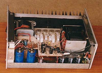
Inside one 50W monobloc. The PSU toroidal power transformer is
under choke at left rear, 2 x 4,700uF
at left front, circuit board and mosfets at rear centre with more
electro C, 3 x 15,000uF caps right front,
and 5Kg OPT with C-cores at right rear. The wide bandwidth OPT has
GOSS double C-cores, build
up total T = 38mm, strip width S = 55mm, window L = 58mm, H =
19mm. These C-cores were made by
AEM in Sth Australia before they ceased C-core production,
and were aimed at the market to be a
replacement for wasteless pattern E&I lams with 38mm tongue
size. I measured the maximum µ for the
C-cores was not more than 4,500. This was sufficiently high to
give cool core running mains transformers,
and quite adequate for any OPT. Not all C-cores from AEM had µ max
4,500, some I used in a tubed
5050 amp
measured µ > 10,000.
Fig 2. OPT-MF1, all details.
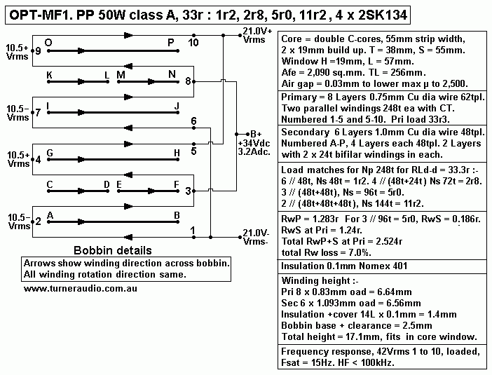
The C-core Afe = 38mm x 55mm = 2,090sq.mm. Better would be E+I
square section Afe with
44mm stack x 44mm tongue. With 42Vrms across primary for 45W of
class A into RLd-d = 35r0,
Fsat occurs at 13Hz. The OPT is about the same size as for a
well designed 50W OPT on a tube amp.
The OPT P : S ratio = turn ratio = 248t : 96t = 2.5833 : 1. ZR =
6.674 : 1 for load ratio 33.4r : 5r0.
As arranged with 0.7Adc for idle Idc to each mosfet, max class A
is with 47r : 7.0r Sec load.
Primary has 8 layers each with 62 turns of 0.75mm Cu dia wire
OPT, arranged for two parallel windings
= 248t, each with a CT taken to +34Vdc. Ends of windings are
taken to mosfet drains. Secondary has 6
layers each with 48t of 1.0mm Cu dia wire arranged for 3
parallel windings of ( 48t + 48t ) for Ns = 96t,
with one end taken to 0V, and other end to active output and for
GNFB to best suit 5r0, but also suit all
loads above 3r0. The OPT bandwidth for 40W class A with plenty
of interleaving is 13Hz at Fsat to
300kHz. Total winding loss = 7.0%.
Original max µ of C-cores from AEM was 4,500 and slightly too
high, although max Lp = 3.3H.
Therefore, with pure class A Pri load of 47r, the XLp 3.3
H Rd-d = RLd-d 47r at 2.26Hz.
The Lp is far higher than it really needs to be. Core could be
fully saturated at Bdc = 1.4Tesla at Idc
across coil = 0.2Adc. This is unlikely with mosfets which do not
change their characteristics like
vacuum tubes.
Anyway, I put plastic air gap material = 0.03mm for gap =
0.06mm, and Lp reduced to 1.7H, which
I think reduced µe to 2,200.
The onset of saturation at 40Vrms across Pri is 12Hz, and the
sudden increase in saturation currents was
less with slight air gap and I doubt increasing air gap any
further would help reduce saturation.
In theory, XLp could be 47r at 14Hz if Lp = 0.53H, and µe could
be 722, so core becomes like something
used for an SE amp. For low RLd-d of say 20r for 3r0, the XLp
0.53H = 20r at 6Hz.
After some consideration, I doubt there is much improvement I
could make to the OPT for the
Sec load range above 3r0.
High saturation currents in OPT could solid state devices to
fail but I have current limiting to less than the
current rating so the fuse should blow first before the mosfets.
Using an air gap with C-cores in a PP OPT opened my mind to
using "partially gapped" cores for any PP
transformer using E+I laminations.
In 1955, most GOSS E+I laminations had a maximum µ = 4,500 when
maximally intermeshed.
During late 1990s I found GOSS E+I was being made with max µ =
17,000.
I used this material in a couple of tube amps before realising
that the material saturates easily if the dc in
each half of the primary is unbalanced, or there are very low
frequency signals across the primary.
But in all these amps there was good monitoring of Idc of each
of multiple tubes, so there was never
ever any use where saturation could occur.
E+I lams may be given partial gapping by arranging all the Es
and Is in sub-packs of say 10E+10I all facing
the same way.
Each pack of 10E and 10I are then inserted into the bobbin hole
for cores in alternating directions.
But to get it right, the core material µ must be measured with
the partial air gapping by applying say 50Vrms
of say 50Hz across primary winding and measuring winding current
to get the 50Hz reactance from which
inductance may be calculated and then µ with gapping may be
calculated because turns, Afe, voltage and
Bac are all known. This is the sort of thing manufacturers
hardly ever bothered to do. The results of the
measurements allow the µ to be adjusted by changing the number
of laminations sub-pack.
Toroidal cores can have max µ = 40,000 and are even more
unsuitable if there is unbalanced DC so they
have no place at all for PP OPT in tube or SS amps. Cambridge
Audio made a stereo amp with toroidal
OPT and it has normal anode load of 3k2 and had B+ of +600V, and
it soon gave nothing but trouble to
its owner and I completely re-engineered the amp after removing
all circuitry Core saturation was one of
many design errors.
Modern C-cores made after 1995 can have max µ > 12,000 if the
joins between C have been polished.
A reduction of max µ to give effective µe by use of an air gap
is best way to achieve low Bdc in C-cores
for PP amps unbalanced Idc.
The air gap size is usually quite low to get µe < 3,000.
Primary Lp PP OPT with balanced Idc can be far higher than
needed without any air gap. For most PP
amps, XLp should equal primary RL at 10Hz or lower, and Fsat
should occur below 14Hz at the Vac that
gives clipping at 1kHz.
The only way to reduce Fsat is to use bigger Afe or have more
primary turns, or both. The size and weight
must increase if the total winding losses are to be kept
constant to say < 7%.
I did think of using 4 x 2SK134 in parallel SE mode which means
the maximum Po is for one load value
only. If I had used above conditions for PP with Ed = +33Vdc, Id
= 0.7Adc, and RLd for each = 47r,
then the 4 mosfets would need OPT for say 11.7r : 5r0, ZR = 2.35
: 1, with TR = 1.53 :1.
Vds = 21Vrms. At OPT sec, Po = 4 x 9.7W = 38.8W to 5r0, Vo =
13.9Vrms
For any load above of below 5r0, the available Po declines with
SE amps. The PP amp has decline
of Po as the load increases, but has increase of Po with
decrease of load because mosfets work in class AB.
But I think for 4 x parallel SE mosfets you could have Ed =
23Vdc and Id = 1.0Adc.
Max Vds = 14Vrms and Iac = 0.707Arms so RLd = 14V / 0.707A =
20r0.
With 4 x 2SK134 you would have RL = 5r0.
To deliver Idc to drains there can be a choke if about 100mH for
4Adc between B+ and drains,
Output is from drains to load via 10,000uF cap. It is a version
of choke feed.
Choke would be similar size to OPT-MF1 or larger.
Even better is to use mosfets in source follower mode with
drains at +23Vdc, and have 1 : 1 OPT that
would be larger than OPT-MF1. This avoids the coupling cap. The
high amount of local series voltage NFB
that is inherent in source follower mode should give the 38W
with THD < 2%.
12dB of GNFB should reduce max THD to 0.5%, as good as many good
tubed SE amps.
The Secondary should always allow for various linking patterns
to keep the mosfet load the same for
say 4r0 and 8r0 at Sec.
I'll leave readers to decide whether 4 x SE mosfets can
work well using a choke or 1:1 OPT and be
equal to the good performance of SE32
or SE35 with tubes.
----------------------------------------------------------------------------------------------------------
MORE ON 2SK134 MOSFET OPERATION.
Above, I said I measured 2SK134 to have :-
Amplification factor, µ = 180 to 200, Dynamic drain resistance,
Rd = 257r to 220r approx.
Transconductance, gm = 0.7 to 0.9 Amps / Volt.
The µ, Rd, and Gm vary considerably between Id min = 0.0A and Id
max = 2Apk.
The region of interest is the low power operation where Id
varies less than +/- 10%
2SK134 has very high gate input resistance like a tube but Cg-s
= 600pF. Cg-d = 11pF which can
to about 210pF if gain = 19 for high class A RLd.
Driving mosfet gates needs a low resistance Vac source lower
than for a tube grid. The source output
resistance at Q1+Q2 collectors is determined by collector loads
of 4k7 to B+ and the ratio of this R plus
the gm of Q1+Q2 to the amount of C to be driven is just as good
as in the best tube amps. The Vg-s
required for the output mosfets is quite low and for the 47r
pure class A load shown in Graph 1 above only
1.0Vrms is needed to make Vds = 21Vrms. The mosfet gain is about
21.0.
Cg-s = 600pF, and Miller C = 210pF for total Cin = 810pF.
But I have each driver bjt driving two gates so Cin = 1,620pF
and if the source R = 4k7, -3dB pole is
at 21kHz, and 4k7 // 1,620pF = 3.3k, but if Vg-0V = 1.3Vrms, the
Iac = 0.39mArms. At 100kHz,
4k7 // 1,620 pF has load = Xc = 981r, and for 1.3Vrms the Iac =
1.33mA = +/-1.875mA, which is low
% of the 6.4mAdc idle current Id of Q1 and Q2.
Thus mosfets are fairly easy to drive in common source mode, and
there is low gate input current at
audio F. ( With bjts in output stage, the base input resistance
is very low and difficult to drive unless you
have a Darlington Pair connection. )
At LF where capacitance reactance does not matter much, the
mosfet may be considered a like an EL34
pentode. The mosfet Rd curve shapes are like the Ra curves for
EL34 pentode, but mosfet currents are
20 times higher and voltages 1/20 of the EL34. Both tubes and
mosfets are equally effective to convey
good music to our ears, but the mosfet cannot be wired as a
triode where there is an internal shunt NFB
network formed by electrostatic field change by anode in series
with opposite field change created by grid.
The triode can be extremely linear without external loop FB but
the pentode and mosfet cannot be.
Consider 1 x 2SK134 with constant Pdd = 23W, Ed = +33V and Id =
0.7Adc. You should get about 10.3W
in SE class A, ( about same as 1 x EL34 ) but mosfet gives
22Vrms to RLd = 47r.
Gain of mosfets.
From Graph 1 and Graph 2, Rd for Egs and Gm are :-
1V, Rd = 2k0, Gm = 0.6A/V,
2V, Rd = 930r, Gm = 0.72A/V,
3V Rd = 233r, Gm = 0.74A/V.
At idle Id = 0.7Adc, and Egs = +1.5Vdc, Gm = 0.7A/V and Rd is
probably 1,300r.
At class A idle condition, Gain A = Gm x ( RL // Rd ) so for RLd
= 47r, A = 0.7 x 45r = 31.5.
But from Graph 1, Vpk-pk for 47r = 63V and Vgs swing = 3Vpk-pk
so gain = 21.
This shows the gain change due to non linearity for the wider Vd
swing.
Do not worry, because there will be a total of 20dB+ loop NFB
from the two types of NFB in the amp.
There is balanced shunt NFB R networks between drains and
collectors of Q1 and Q2. The amount of
shunt NFB varies during each wave cycle but is about 12 dB
minimum and the amount of GNFB then
remains fairly constant at 15dB for the loads shown in Fig 1.
Fig 3. Most basic shunt FB model.
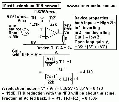
Fig 3 shows the most basic shunt FB with R1 + R2 network between
output of an amp and input voltage
source.
In this example, the triangle amp has gain = 24, and the figures
show the the results. But without knowing the
Rout of devices in triangle, we cannot calculate Rout with NFB.
Such basic model diagrams usually assume
the device is an op-amp, but it could be a single tube or a
mosfet etc. Inputs 1 and 2 are assumed to be
high Z, but in fact input may be low Zin if it is a cathode or
source or emitter. Correct working can only occur
if input 1 is high Zin.
Fig 4. Model of 1/2 the amp used in 50W monobloc in class
A.
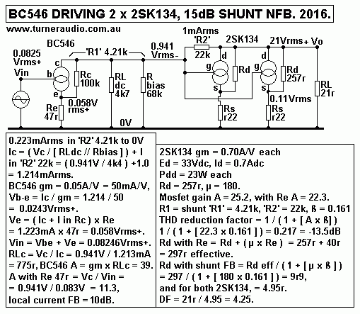
Fig 4 shows 1/2 the schematic in basic model form of Fig 1
schematic. BC546 and 2SK134 are shown as
"voltage controlled current generators", the double Os, with
high input Z and infinite Z between c to e, and
d to s, with a finite amount of shunt resistance Rc, Rd which is
appears strapped across the internal device
and which can be seen in data sheets where Rc or Rd curves are
slightly sloped up from low Ec or Ed
toward the right. The base to emitter input resistance of BC546
has been ignored, but would be over 5k0
and the Vac source resistance of base input signals < 50r.
Instead of having shunt NFB network with 'R1' + 'R2' between
input voltage source and output, 'R1'
is the total of parallel resistances Rc // RLdc // Rbias =
4.21k, and are between mosfet gates and 0V.
'R2' is 22k between mosfet sources and gates. The BC546 with
high output Rc resistance supplies
current to the junction of 'R1' and 'R2' which is the gate. Any
THD voltage at drains is divided by the
R network ß fraction = 0.161, and appears at gates to be
amplified by mosfet gain x 22.3 to make
a correction signal to subtract from the THD which appears
before any NFB is applied.
If you measured distortion Vdn at drains = 0.21Vrms+, then Vdn
at gates = 0.0338Vrms+ which is
amplified x 22.3 to make a correction signal = 0.754Vrms-, which
we cannot measure. The Vdn which
exists before NFB is applied = ( calculated correction Vdn +
measured Vdn with NFB ) = 0.745V + 0.21V
= 0.96Vrms+.
The NFB reduces THD by factor of Vdn with NFB / Vdn without NFB
= 0.21V / 0.96V = 0.217
= -13.5dB.
The full exact model of a bjt is more complex than I have shown,
but what I do show is enough to
do the analysis to grasp the fundamental mental concepts.
The effective collector resistance Rc for Q1 BC546 cannot be
accurately known unless it is measured,
but a view of static curves by someone with curve tracer showed
BC546B had Rc > 80k at Ic = 7mAdc,
and Ec = 20Vdc, about as I have Q1+Q2.
Typical small bjt Gm = 0.05A/V, so that µ > 4,000, and with
re = 47r, the effective Rc > 250k.
Most ppl do not consider the ideas of gm and µ apply with bjts,
and they want to discuss all in terms of
hfe, ie, relative currents of base and collector, and that is
all very well, but the fact remains that you need a
voltage applied between base and emitter to make anything Vc
appear, and the old fashioned tube terms
can be universal.
I found it safe to assume effective Rc = 100k, and calculate
results which may be better in a real circuit.
Being totally exact with the figures for all these sorts of
analog circuits is dreadfully tedious, and it is almost
impossible to get analysis to be 100% correct, and then find the
next fellow with IQ 269 is happy to spend
2 months to work out that you were right by a factor of only
97%.
What I offer is enough depth, rather than none at all.
The global negative feedback network, GNFB is a generic sample
of "series voltage NFB."
Fig 1 amp schematic has 0.65Vac applied as GNFB from OPT sec to
base of Q1 bjt in the input
differential pair.
For the Q1+Q2 collector Vc as shown, required base to base input
is about 0.12Vrms. Therefore the
base input to Q2 = 0.65Vrms NFB + 0.12Vrms = 0.77Vrms.
Gain reduction factor with GNFB = 0.12V / 0.65V = 0.18, or
-14dB.
Total NFB is shunt NFB and GNFB = 13.5dB + 14bB = 27.5dB. This
is quite enough total NFB to reduce
THD, IMD, noise, and Rout to levels only found from the best of
amps.
Heat dissipated in mosfets in class A is always a worry because
they run warm or even hot even with no
signal at idle. But they get slightly cooler once music signals
are amplified because some of the Pdd heat
at idle is converted to audio power. Under most conditions where
average AF Po is 2W, and
the idle power of mosfets is 100W, the the Pdd is at average of
98W, and there is no insignificant change
of temperature.
Heatsinks should always be chosen to handle more heat than any
theory might say is OK.
My theory suggests a few things :-
1. Do not ever rely on a fan, or build any hi-fi amp with a fan.
That is because fans always make noise,
and what happens when the fan ceases to work for one of many
reasons?
2. All hi-fi amp heatsinks must have vertical fins, and with no
restriction on a free flow of air up past the
fins. Where ever possible, the flat vertical inner surface of a
heatsink should have ventilation from
many holes in bottom plate cover and up through holes in the top
of sides of amp box.
3. The total surface area of the heatsink including both sides
of all fins and inside flat surfaces must
be at least enough to have 40 square centimetres, or 6.25
sq.inches per watt of heat likely to be
produced even in a fault condition.
4. Temperature rise above ambient should remain less than 20C.
It means that if the room temp is 25C,
quite warm, then heatsink should go no higher than 45C, and you
can place a hand on that without being
burnt, but you won't want to keep your hand there.
Above, I have said we would have Pdd for one 2SK134 = 23W, and I
suggest heatsink size area Ahs
be OK for 30W, so Ahs for one mosfet = 30 x 40sq.cm =
1,200sq.cm, and for 4 mosfets Ahs
= 4,800 sq.cm.
Best heatsink for this type of amp is from Conrad Heatsinks in
Melbourne.
http://www.conradheatsinks.com/products/
http://www.conradheatsinks.com/products/conrad-catalogue-05.pdf
See the MF35-151.5 Its 350mm long, x 151mm high and has thermal
coefficient of of 0.21, and best
suits flat pack TO3P style mosfets simply screwed to flat
surface on one side away from fins on the
outer side.
There are 35 fins of 40mm long x 150mm, with main plate 350mm x
150mm, and total surface area
= 5,250 sq.cm. This HS is longer and taller than on my amp and
you really need more internal volume
than I used for each 50W mono amp. I have 4 x 2SK134 bolted
beside each other on a 12mm AL
angle ledge which bolts to center of a home made HS from scrap
AL I had accumulated. T rise = +25C
above ambient and because mosfets are clustered in center they
make the central portion of HS hotter
than it would have been had the mosfets been spread out evenly
along the HS length.
I have a pair of M35-151.5 ready for use with the next mosfet
amp I make.
Meanwhile, I don't want to change much in the amp I already
have, and I don't ever use 50W, and all
is OK if the first 20W is pure class A and remainder is class
AB. I have found Pdd of 23W is OK
with Ed = 33Vdc and Id = 0.7Adc.
Nelson Pass once promoted a simple mosfet amp which used Ed =
+17Vdc with Id = 3Adc, and with
ONE mosfet and with Pdd = 51W. A friend of mine tried to build
this 'Zen' amp and after smoking 3
expensive IRF mosfets due to inexplicable "smoke and silence"
events he gave up and has never
found the time to learn more and complete the amp. From Pdd of
51W, some 17W of SE class A
was supposed to be available for RL = 3r8.
Take my word for it, 30W is the absolute limit for idle
dissipation in any flat pack or TO3 devices !!!!!
The noise was slightly too high without GNFB. But the GNFB
reduced mosfet noise to negligible levels.
Rout measured 0.2r with GNFB, THD < 0.2% at -1dB below
clipping, and declining towards zero as the
Po was reduced. I could not see any sign of crossover distortion
or core distortion.
The amp needed zobel networks across the collectors of the
driver LTP, and across each half of the
OPT to shelve the HF gain and control phase shift the same way
as a tube amp would need.
The OPT has a full power bandwidth from 10Hz to 300kHz, ( not a
typo ), and this much bandwidth
cannot be used, and could lead to RF oscillations. To control
overshoot on square waves with capacitor
loads above 40kHz the shelving networks were employed and so the
final finished bandwidth is a more
sensible 10Hz to 65kHz, with pleasing looking 5kHz square waves.
About 99.9% of mainstream solid state amps do not use an OPT. I
have proved to myself OPTs can
be used effectively. My mosfet amp has the ability to get a good
load match even to 3r0, and still
get a large amount of class A Po, always good for the music.
Since all the output devices are NPN
types with the same part number, any even number H products on
each side of the PP circuit cancels
almost perfectly. The circuit doesn't need an intermediary high
gain voltage amplification stage.
Instead of having a single phase of drive signal applied to a
complementary PP pair of PNP and NPN
devices, the two output phases of the input differential amp are
both used. The difference between
PNP and NPN devices when in common source mode is substantial,
equivalent to having an EL34 on
one side of a tube PP amp and a 6L6GC on the other; it does not
give the best outcome.
------------------------------------------------------------------------------------------------------------------------------
Future possible improvements. I did think about use of
using a pair of matched darlington pair
connected bjts for the differential input/driver LTP to increase
local open loop gain and give better
linearity and to increase the input impedance of the amp
slightly. But then I realized I would still have
bjts at the input, so would they sound better or measure better?
I doubt it.
Then I thought of using 2SK369 j-fets for LTP diff input plus
its CCS for commoned sources to give
an amp with only j-fets and mosfets. 2SK369 has nearly same
specs as 2SK147, now no longer made
by Hitachi. 2SK369 has slightly lower Pdd rating of 0.4W. With
Ed +15V and Id 8mAdc, Pdd = 0.12W
so they would survive without needing heatsinks. 2SK369 will
work OK with same idle currents as I have
in bjts Q1+Q2, but Ed could be lower at +15Vdc. 2SK369 has very
high input impedance gates and produces
far less noise than any bjt at Id 7mAc. The gm = 40mA / V at 5mA
of idle current and would suit this amp
very well. I doubt much change to sound, but Hoo Iz Tanoe unless
someone tries it?
Most PP tube amps have schematics just as simple as my 50W
mosfet amp. The simplest PP will use
2 input tubes to drive 2 more output tubes. Quad-II with 2 x
EF86 driving 2 x KT66 is a perfect example.
Consider 4 x 2SK134 in balanced source follower mode to drive an
OPT and with Ed +33Vdc,
Id 0.7Adc and class A load = 24r, with Re 0r22. Open loop gain =
25.2, with Re it is 22.3, and source
follower connection reduces A to 22.3 / ( 1 + 22.3 ) = 0.961, so
A reduction with the follower NFB
= -27dB, and THD is reduced by same factor, and it is 13.5dB
more than use of 13.5dB of shunt NFB
so far explained. One might expect 5% THD in class A with no NFB
at all, but with 27dB, this is reduced
in theory to 0.21% at just under clipping at say 38W. We could
expect 0.05% THD at 2W.
GNFB from OPT sec to one of two input ports at input pair is not
absolutely necessary as long as we
can produce a low THD drive signal of up to 22Vrms max to each
2SK134 gate.
The 2SK369 would never be able to do this job, IRF610 with idle
current of about 50mAdc in each
might just do the job, but nowhere near as well as a pair of
EL84 in triode mode, or a pair of ECC99.
I have found EL84 in triode in LTP can produce astonishingly low
THD even when asked to produce
up to 80Vrms at each anode, as I have done at my 8585 and 300W
tube amps.
Fig 5. Basic triode PP input to drive mosfet gates.
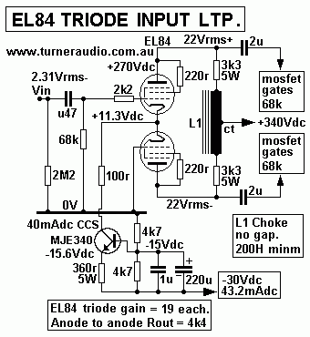
Fig 5 shows a very simple EL84 triode LTP with MJE 340 CCS to
give fairly well balanced Va
to drive mosfet gates.
The idea can be taken further to include NFB from mosfet sources
to the screen grids of EL84.
Fig 6. EL84 input/driver to mosfet output stage, balanced
screen GNFB.
Most explanations of function are on the Fig 6 schematic. Screen
g2 gm = 0.4mA/V and the g2 gain is
calculated at 50Hz as gm x ( RLa // Ra ). There are 2 parallel
loads plus Ra :- gate bias R = 68k,
impedance of 3k3 in series with 1/4 of the total of all XL1 =
75k, Ra of EL84 at 20mAdc, 100k, so
resultant total = 26k. Screen g2 gain = gm x total RL = 0.4 x 26
= 10.4.
This is just over 20dB.
I estimated 18dB. THD at 2SK134 sources at max class A is
estimated at 0.33%, and all is fed back
to screens so ß = 1.0. THD is reduced by factor of 1 / ( 1 + [ A
x ß ] ) = 1 / 11.4 = 0.087, or by more
than 20dB, so we may expect THD to be 0.033% at 44W class A.
However, the EL84 will have some
slight 3H of up to about 0.03% at 20Vrms while working into
loads of 75k//68k ie 35k, which is 14 times
triode Ra for EL84 so I can forecast THD of the amp > 0.1% at
44W.The only unbalanced function in
the amp is at input where V2 grid is grounded, and Vin is
2.6Vrms atV1 grid. This means commoned
cathode have 1.3Vrms, and Va-k for each tube is slightly
different.But where there is a constant current
sink to both cathodes, and RLa in each are equal, the Va of each
EL84 will be balanced within 1%, and
the so so will be the production of the balanced error signals,
and any possible imbalance will be
corrected by the NFB action. The only way for me to verify that
this schematic will work is to build it!
I can most certainly say that nobody would be able to simulate
this schematic properly.
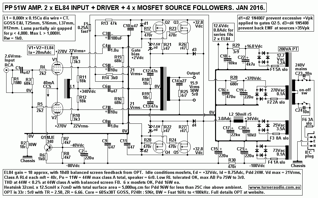
The PSU for the Fig 4 schematic is a little different to that in
Fig 1 above because there must be a
+370Vdc supply for the EL84, and I also show them with 12.6Vdc
to heaters, so I will have to replace
the toroidal PT which I used before 2000 when I built the 50W
mono amps.
--------------------------------------------------------------------------------------------------------------------------------------
The original PSU from 2000 uses CLC filter for +33Vdc rail with
C15 = 2 x parallel 4,700uF,
L1 = 15mH, Rw < 0.5r, C14 = 3 x parallel 15,000uF. At 3Adc,
Vripple < 4mV, but there is some common
mode LF noise due to mains level changes. The PP excludes most
common mode noise. The resonant
Fo for 15mH and 45,000uF = 6Hz, low enough.
The toroidal PT has one HT winding with 27Vrms each side of CT
for the +33Vdc rail. I added turns to get
47Vrms each side to give +/- 65Vdc which is RC filtered down and
shunt regulated with Zener diodes for
+50Vdc and -33Vdc for Q1+Q2+Q3. The amp is not troubled by wide
variations in the mains voltages.
Between 2000 and 2016, nobody has complained about the sound
which they found little different to the
best class A tube amps. I did run blind A-B tests and nobody
could distinguish the difference when speakers
were switched from mosfets to tubes, with both amps having
accurately preset input levels for equal Vo
and from the same preamp.
Should anyone never want to use CLC filtering or OPT they could
settle for a complementary pair PP output
stage and driver stage similar to my 2X300W AB stereo amp.
This has 3 x 2SK1058, npn, and 3 x 2SJ162, pnp
mosfets.
Supply rails are +/-70Vdc with 50Vac each side of CT on PT.
The supply rails could easily be reduced to +/- 35Vdc, and all
Ed about +34V, Pdd 17W at idle, Id = 0.5Adc.
Total Pdd for heatsink = 102W, quite OK for the heatsink size.
Class A RL for each 2SK1058 = 60r, and the
6 mosfets work in parallel on 10r0 for 45W pure class A. But
with 5r0, Class A Po = 22.5W, with class AB
at 88W, and this would please the vast majority of listeners.
I once did a blind A-B comparison with 4 gathered friends in
1996 and none could tell any difference between
the 2x300W in its original form when compared to an 8585 with 4
x 6550 per channel and OPT.
They didn't like me trying to trick them but they ended up
agreeing that the "...same bastard built both bloody
amps so both amps sound good..."
So they didn't want to hang me on the tree outside, and I made
them all a cup of tea.
In 2001, one of the guys could not tell the difference between
the 50W mono amps and a 2 x 100W tube amp.
There are 1,001 ways to build an amplifier.
-----------------------------------------------------------------------------------------------------------------------------------------
For more simple ideas with mosfets and OPT go to Susan Parker's
website at
http://www.audiophonics.com/audiophonics-zeus-about.html.
She has some excellent ideas to consider, and has measured
performance of modern mosfets in PP class A.
The PP connection with the same NPN devices instead of the
normal complementary pair with both P and N
devices gives much less THD.
With source follower configuration, the OPT primary has CT to
0V, and the OPT can then be an auto-transformer
with taps each side of CT for a number of pairs of connections
to suit say 2r0, 4r0, 8r0 or 16r0.
There is no need for an isolation transformer, but the auto
tranny must still be wound to have its 4r0 windings
well interleaved to get good HF response; the auto-transformer
is more difficult to optimize and the isolation
transformer can be better for HF, but then I have thought a bit
longer and I wrote a page at
http://www.turneraudio.com.au/output-trans-speaker-matching.html
I have also thought of using the Circlotron connection which has
the advantage of grounded windings in the
source circuits, and drive to gates < 11Vrms, and the NFB in
output stage is still just over 20dB.
Back to Index Page.
Fig 7. 2SK134 Blank sheet for drawing load
lines.......