CHOKES - PAGE 2.
This page 2 is about........
1. Filter chokes for "choke input" or LC filters in power
supplies.
Fig 1, "Traditional" 2011 choke input + rectifier + following LC
filter,
Fig 2, "Modern" 2011 choke input + rectifier + following RC
filter,
Fig 3, Other 2007 choke input + rectifier + LC filter.
2. Design Method for Choke in LC PSU, steps (1) to (20),
Table 1, Wire size table for sizes of available 200C temp rated
polyester-imide magnet winding wire.
Fig 4, "Wasteless pattern" E&I lamination size relationships
& details for L, H, T.
Table 2, Properties of chokes with T32 and S = 6.3mm to 64mm.
Other related pages :-
Basics about inductance and chokes, inductance test circuit,
Comparison of CRCRC
filters with CLC filters, Choke Design Method for CLC filter, go
to Chokes 1
For chokes used for dc supply to anodes, cathodes, go to Chokes 3
-----------------------------------------------------------------------------------------------------------------------------
1. Choke input power supplies.
Choke input power supplies also known as LC input supplies have
been the best old fashioned
or traditional way to build a Vdc rail supply, especially where
the current draw will vary by a factor of
10 or more as is the case with a power supply for a class AB, B or
C amplifier.
A "choke input" basically has a HT winding with CT followed by two
diodes, or a HT winding
with a four diode bridge with diodes connecting to a choke in
series with a capacitance shunting
a load where Idc changes during normal use. The choke usually has
more maximum inductance and
is larger than used in a CLC type of filter, but also has low
winding resistance.
Rectifiers for high voltages were usually vacuum tube or mercury
vapour diodes with limited peak
current abilities but with very adequate reverse voltage
tolerance. With the advent of silicon diodes
which cost 1/100 of a tube rectifier, the choke input PSU has
become fallen from widespread use
because of the cost savings possible by not using large heavy
input choke and vacuum diodes.
Modern high value capacitors are now very cheap and reliable.
However, I sometimes found the choke input supply to provide a
solution where one wishes to use
a HT winding of a given transformer where otherwise the B+ Vdc
gained by Si diodes charging a
capacitor directly would be much too high.
Fig 1. Traditional choke input PSU also with added LC
filter.
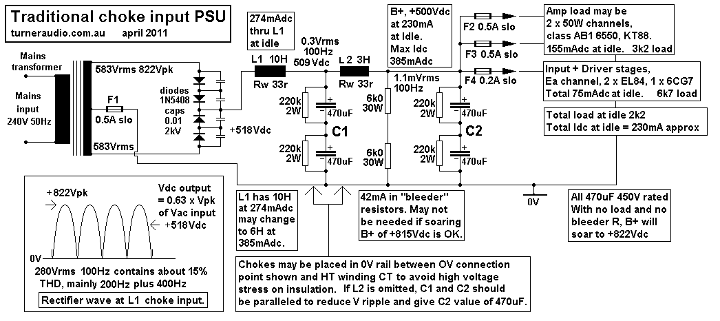
Fig 1 shows diodes charging capacitor C1 with continuous current
through L1. L2 + C2 filter the B+
output which feeds the two OPT in a stereo amp with two 50W
channels with 6550 or equivalents.
The L1 + C1 form a simple a second order filter with low F pole at
3.3Hz, which is also the Fo for the
10H and 235uF. L1 is designed to have inductance = RL / 900 in
Henry where RL = B+ Vdc / Idc minimum
which in this case 44mA, So minimum RL = 11.4k so max L = 12.6H.
As Idc increases to a possible maximum of 385mAdc, the L1
inductance should decrease to about 6H.
This choke L1 is known as a "swinging choke". At the idle current
of 230mAdc, expect L1 = 10H.
L2 is a smaller choke to provide additional filtering at C2. The
Fo of L2 + C2 = 6Hz. There is no
added resistance between L2 and C2 to provide damping of 6Hz
resonance signals. The load at
the output of tubes plus bleeder resistance of 12k0 is not low
enough to provide Fo damping.
Resonances at 3Hz from L1 + C1 will also appear at C2. Amplifier
gain will be -3dB at 10Hz and
-12dB at 5Hz, so the amplifier will not excite much resonance at
C2. The slight very low frequency
ripple in the B+ rail will not cause much IMD because the PP
output stage has good CMR for signals
applied to the OPT CT.
The HT winding plus diodes establish an ac voltage of mainly 100Hz
with even order harmonics
plus a Vdc content of 0.63 x Peak voltage of HT Vac. This is the
*average* voltage present of the
100Hz V peak to peak which sits above the 0V rail as shown in the
bottom left wave diagram.
The HT winding is a 583V - 0 - 583V winding with CT and each side
of the CT primary delivers
60VA of power to make a total of 120VA delivered to L1 choke.
+822Vpk is produced after the
diodes at L1 input. There is approximately 280Vrms of 100Hz signal
applied to L1 input with about
15% of even order THD product. The L1+C1 and L2+C2 filters allow
the LF content below 6Hz
and DC current to flow through to the amplifier load while 100Hz +
harmonics are blocked by the
choke's high reactance at 100Hz, and while low reactance of C1, C2
shunt the signals
above 6Hz. The +500Vdc at 230mAdc at C2 will drop to about +485Vdc
at Idc of 385mAdc if
we estimate the PSU resistance before the amplifier is a total of
100r. The choke input filter gives
fair regulation of the B+ output voltage where the current may
vary from the idle condition to 2
times the idle current. Regulation depends on transformer and
choke winding resistances and
diode resistances. The high peak current charging of the CLC
filter do not occur. The diode charge
current flows continuously, so power dissipated in the HT winding
is 30% less than in a typical
CLC supply providing the same VA. If no tubes are connected, the
only Idc flow is the 44mAdc
through the bleeder resistance but this keeps the max Vdc at C2
down to about +540Vdc.
The choke input supply ripple voltage will be higher L1 + C1 for
the same amount of total L and C
used in a C-L-C filter. Despite its limitations, choke input
supplies have admirers because the
continuous current flows do not produce switching pulses around
ground paths and transformer
windings remain silent. The available HT supply voltage at the
power transformer suits a wanted
lower Vdc to be produced. The regulation possible with tube diodes
is acceptable and the tubes
do not exceed their limited current ratings. In this example I
expect to get 500Vdc from a 583Vrms
transformer winding which is a Vac to Vdc conversion factor of
0.86. In practice, due to winding,
I would be lucky to see exactly what I have shown above.
The function of the bleeder resistors of 2 x 6k0 ensure Idc =
approx 44mA without the amplifier
connected. The B+ voltage may rise to about +540Vdc when Idc =
44mA. But as Idc is reduced
further the B+ will rise to the peak HT Vac which is +822Vdc when
Idc = 0.0mA. In fact, without a
bleed resistor, there would be 3.6mAdc through the 220k across
each 470uF capacitor.
All choke input filters will produce a "soaring B+" when the Idc
is very low.
Now the input plus driver tubes plus any other R across caps etc
will draw 75mA for both channels
and this is enough current to provide a bleeder current to stop
the B+ soaring even if there are no
output tubes connected. Therefore in this case the bleeder R is
optional, but we would want to make
sure all parts of the circuit will withstand +822Vdc applied until
the tubes warm up and begin to
conduct their idle Idc. To stop soaring B+ even for the short
period after turn on and to avoid
wasting 42mAdc of flow in the bleeder R there could be separate PT
for the tube heaters and
bias supply and this is turned on by the on switch. 30seconds
later the PT for HT is turned
by a delay circuit controlling a relay in the 240V winding. This
would be the most traditional
approach without using the kind of immediately active solid state
bleeder circuit I show in Fig 2
below to better manage the On-Off behavior. Bias failure
protection could be powered by
the twin mains transformer option by turning off the HT if Idc in
any one tube remains above
twice the idle value for longer than 4 seconds.
Fig 2. Modern choke input.
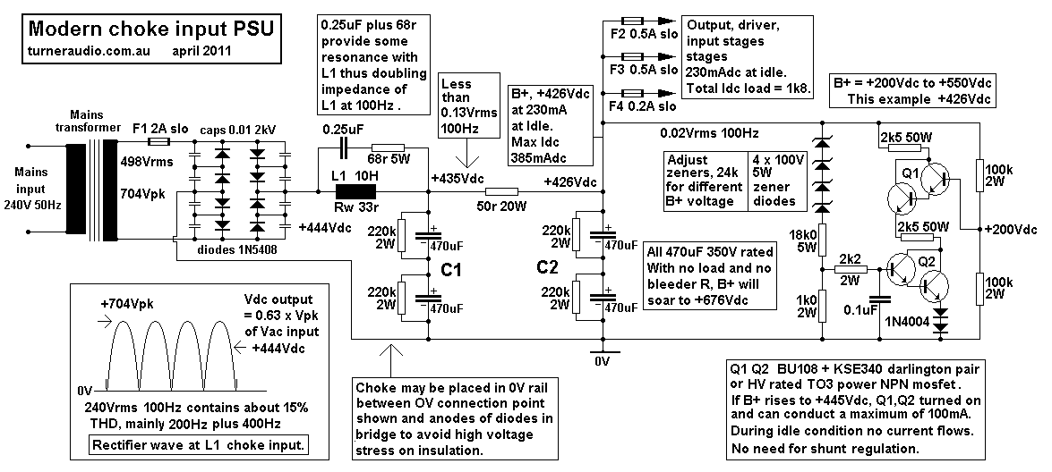
Fig 2 shows a slightly different choke input PSU with slightly
more modern attributes.
The general working is the same as Fig 1. The L1 choke used is
designed to have high inductance
under low current idle conditions, but when current is increased
from 230mAdc to 385mAdc
the B+ voltage drop may only be 17Vdc.
There are some modern tricks used in Fig 2. There is a diode
bridge, very easy with Si diodes,
so the the HT winding uses thicker wire and 1/2 the turns of a CT
winding which is easier to do.
There is also a 0.25uF plus 68r across L1 which causes L1 to about
double its impedance at
100Hz due to damped parallel resonance. The value of 0.25uF is
chosen for the value of the
L1 inductance at the idle current condition. At less Idc than at
idle, the L1 inductance will rise
and Fo will drop below 100Hz, and with Idc at 385mAdc, L1 may be
6H so Fo will move
above 100Hz, but this is no problem because in practice the Idc
will not much change because
most audio power is created by class A action of the OP tubes. But
the reduced 100Hz ripple
reduction is always welcome, and achieved at minimal cost.
There is no need for L2 and 50r resistance will give an
attenuation factor of about 1/6 of V ripple.
The use of the 50r & C2 filter instead of LC filter will
provide damping of resonance in L1 & C1.
The Vripple will be higher than for LCLC type of filter in Fig1,
but Vripple will be low enough at C2.
The input driver stages will have another RC filter for their B+
rails so filtering will be OK.
Q1 and Q2 are a pair of HV rated darlington pair connected
transistors. You could use two HV
mosfets for the same same thing. The SS devices are connected in
series to distribute the high
B+ Vdc rail voltage so the maximum possible Vdc between collector
and emitter is +275Vdc
if the B+ rail was +550V. The 2k5 x 50W rated resistors may allow
a maximum of 100mAdc
to flow through transistors with B+ = +503Vdc and the transistors
will turned on fully and have
very low voltage across them so will be cool while resistors are
hot. If I = 50maMadc, the Pd in
each 2k5 and in each darlington pair transistor = 6.3W.
Fig 3. Choke input LC + LC filter.
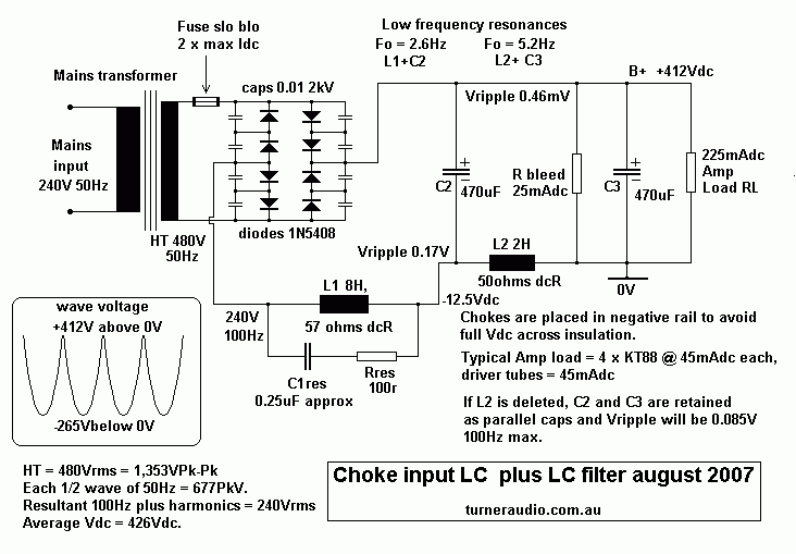
Fig 3 shows a combination of choke input plus following LC filter
in the classic LCLC arrangement
used in many older designs for where tubes operate in class AB
with low bias currents.
However, perfectionists who like quiet rail voltages can use it
for their class AB hi-fi amp with high
bias currents and where Ia does not vary much in practice.
Fig 3 shows the input choke L1 and following choke L2 in the
ground rail rather than in the B+ rail.
I have never found the placement of chokes in the B+ rail to work
any better than being in the ground rail.
Such choke placement means the choke windings are at a slight
negative dc voltage potential and thus
there is less voltage across insulation between windings earthy
core iron. The actual 0V connection
can ONLY be made where I have indicated, or else the benefits are
entirely negated. The wave form
after the diodes and at the input to the L1 choke is indicated,
and is an inverted wave form compared
to when the L1 is placed in the B+ rail.
The ripple voltage at bottom of C2 is less than 0.2Vrms, and if L2
was omitted, and C2 paralleled with
C3, then ripple at B+ would be less than 0.1V, and quite OK for PP
amps.
However, for SE amps 100mV of ripple may be too high, and the two
LC sections are useful although
an RC section after L1&C2 where R = 50r as indicated in Fig 2
usually reduces Vripple enough plus
damps unwanted LF resonance. With SE amps PSU regulation is not
critical because the Idc from PSU
to OPT remains constant.
----------------------------------------------------------------------------------------------------------------------------------------
It is difficult to make a choke for LC input which will be
mechanically quiet. LC input chokes
tend to hum with vibration because of the high amplitude voltage
of twice the mains frequency
plus harmonics which is applied across the choke. So the choke
must not saturate because of the
combined dc current magnetization and the applied ac current
magnetization. This type of choke
should be potted after being very well varnish impregnated to stop
winding or core movements.
Potting will stop most stray radiated magnetic fields and quieten
them. The varnishing is very
important to prevent windings moving because of the high AC
voltage applied.
In 2004, I re-engineered a customer's Phase Linear 700W
transistor amplifier. This amp had
+/- 87Vdc rail voltages which were too high for reliability. The
existing PT was noisy, and heat
sinks seemed far too small. The customer had no need for 700W
capability, but insisted on high
current ability. I wound two chokes of about 0.35H for each + rail
and -rail. These were well
varnished and potted with roof pitch in 1mm sheet steel cube
shaped boxes with a side length
of 90mm. The power transformer had a CT sec winding with 62V- 0 -
62V and there was
a 35A rated diode bridge. I obtained +/- 55Vdc which gave plenty
of power. The PT noise
became negligible. The resulting "Phase Turner" amp has
remained a very fine sub-woofer amp
for the last 7 years so far. Recordings of the Space Shuttle
taking off rattled the windows.
If you insist you want a choke input filter, there are basic
rules.
Minimum critical choke value, Henry = RL / 900. Where
mains = 50Hz,
where RL = Vdc output / dc current at the minimum current.
The choke value is called the critical choke value. Choke input
PSU were often used for class AB
tube amps where the anode input current flowing into the output
stage may have varied enormously.
The current flowing into the C1 reservoir cap through the choke L1
is continuous in each 1/2 wave
cycle. There is no heavy peak charge current over a small fraction
of the wave cycle at the peak of
the wave as there is with a capacitor input CLC PSU. The LC input
allows vacuum tube rectifiers
to be used and in high power and high voltage applications, use of
mercury vapour vacuum tube diodes
such as 866 were good with a following class AB amp of kilowatt
capability. The minimum and
maximum dc current flows must be known, and for some old fashioned
amps the minimum current
is taken to be 10% of the maximum which will be calculated and
become known. With LC inputs
The minimum must be allowed to flow even when output tubes are
biased right off, as in the case
of a real class B or class C RF amp.
Unless there is some minimum current flow which is called the
"bleed current", the B+ Vdc can
soar to the full value of 1.41 x the HT winding Vrms voltage,
possibly stressing other components or
insulation layers especially if the DC voltage exceeds 1,000V when
corona effects can start arcing
in amplifiers.
In about 2005 I completely re-engineered a very poorly designed CR
Audio Developments
"Woodham" 5050 stereo amp with a pair of PP channels with KT88.
The original amp had HT
transformer voltage of 487Vrms and the cap input with Si diode
bridge gave up to +650Vdc.
This powered a very poor imitation of the McIntosh style of output
stage. One could only get 40
Watts of audio for a short time before smoke arose from this
horrid amplifier. The anode to anode
loading was found to be about 1/3 of the correct value for such a
high B+ voltage.
I found I had a choke which could be suitable. So after a few
tests I potted it and got B+ of +430Vdc
at the at the reservoir cap after the choke at full current draw.
I converted the amp to 50% UL
because the toroidal OPTs had 4 primary windings which could be
re-arranged. I got 45 reliable
Watts at about 1/5 of the THD/IMD and better damping factor with
revised loading for the OPT etc.
I made a solid state shunt regulated supply for input tubes which
ensures 30mA is
drawn right after switch on so B+ does not rise above +450Vdc, and
as the output stage current
begins to flow to a normal level of 250mA, the shunt regulator
reduces its bleed current "wastage"
of energy, and B+ remains steady at +420V despite the huge change
in current.
In this amp, when Idc = 30mA, RL = 450V / 0.03A = 15,000 ohms. To
ensure the choke would
work with low current to keep +Vdc less than +450V, the choke
should have had a maximum L
value = 16.7H. The choke only had 9H at 30mA. At 250mA, when the
amp load reduced to 1,680
ohms, the choke inductance fell to about 4Henrys due to the heavy
DC flow. The result was that
the "knee" of the regulation "curve"
wasn't sharp, and at low Idc the voltage at the PSU tended to soar
above +500V. With a choke in
a CLC supply, the Bdc can be allowed to be quite high at the
highest Idc, because the Bac is
quite negligible. But in the choke for LC input, the Bac is MUCH
greater, and for most amps we
should make sure Bdc = Bac = 0.6Tesla maximum, for maximum Idc.
Thus the choke for LC
input is always going to be larger than the choke for CLC.
There is a simple remedy for where there is only 1/2 the wanted
maximum critical inductance.
An R+C Zobel network is connected across the choke so that the L
and the C value have a
resonance at the ripple frequency where the L value is slightly
above where Idc is minimum.
I placed a 0.33uF cap plus 100 ohms for a Zobel network across the
choke when its value = 8H,
so that the cap and the L were resonant at near 100Hz. The effect
was quite remarkable,
and this choke plus Zobel acted almost identically to a choke of
16H, or twice what I had,
and B+ soaring was prevented, and Vdc better regulated, and a low
bleed current was required.
So if one wants 250mA maximum, bleed current should be at least
25mA.
For best natural B+ regulation, the power transformer and choke
should have low winding
resistances. If the choke was 50ohms, the change in current of
200mAdc would cause an
unavoidable drop of 10Vdc. This isn't bad, but never use a choke
of 500 ohms! It will
smoke, and regulate poorly.
------------------------------------------------------------------------------------------------------------------------------
2. Design Method - Choke for LC PSU.
Now let us consider the design of a choke L1 in Fig 2 where there
will be +435Vdc at C1, and
300mAdc maximum continuous with LC input filter. Let us design the
choke without reliance
on a Zobel resonant RC network across the choke to improve 100Hz
filtering at low Idc levels.
The Zobel may be added to the circuit upon completion to not only
improve 100Hz noise rejection,
but to provide a resistance load at switching frequencies to damp
diode switching transient emf
which could apply excessively high voltages to the power
transformer insulation. If the maximum
L is available is thus sufficient, and the Bdc at full current
still permits the choke to work as a pure
inductance without ac saturation, the choke is well designed. The
dc current density should not
exceed 2A/sq.mm at maximum Idc.
To calculate wire Cu dia, d :-
For 1A/sq.mm, d = 1.13 x sq.rt Idc,
For 2A/sq.mm, d = 0.8 x sq.rt Idc,
For 3A/sq.mm, d = 0.65 x sq.rt Idc, Idc in Amps, d in mm.
(1) What is the wanted range of DC currents at the nominal B+ Vdc
rail?
What is the range of load values supplied by power from the power
supply?
Idc min = 30mAdc, Wanted B+ at C1 = +435V, Maximum RL = Vdc / Idc
= 14,166r.
Idc max = 300mAdc, Expect Vdc = +425V, Minimum RL = Vdc / Idc =
1,417r.
(2) Maximum allowable Rw = Minimum RL / 30.
Rw = RL minimum / 30 = 1,417r / 30 = 47r.
(3) Maximum wanted L.
L max = max RL / 900 = 14,166r / 900 = 15.7H.
(4) Minimum wanted L.
L min = min RL / 900 = 1,417r / 900 = 1.57H
(5) Maximum Cu current density = 2A / sq.mm, For 2A / sq.mm, Cu
dia = 0.8 x sq.rt I, d in mm, Idc in Amps.
Cu dia = 0.8 x sq.rt 0.3Adc = 0.438mm.
(6) Select wire size from table......
Table 1. Wire sizes.
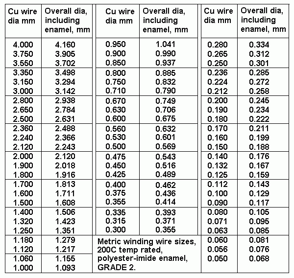
Try 0.45Cu dia , o/a dia including enamel = 0.516mm.
(7) Select T dimension of E&I wasteless laminations.
Fig 4. Relative dimensions of T, window L and H and plan oa
sizes, bobbin winding areas.
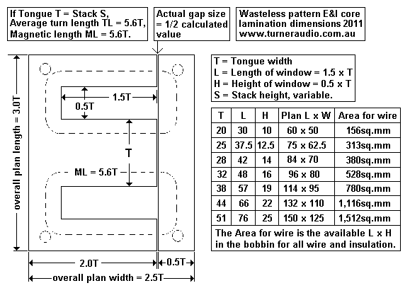
Try choosing T = 32mm.
(8) Read table for area for winding wire, Winding Area = 12mm x
44mm = 528 sq.mm.
Note. 32T core window L x H = 48mm x 16mm = 768sq.mm, but area for
wire in bobbin
= 44mm x 12mm = 528sq.mm.
(9) Calculate Number of turns N = WA / oa dia squared, for coil
without insulation layers.
N = 528sq.mm / ( 0.52mm x 0.52mm ) = 1,950 turns.
(10) Calculate Turn Length TL = Rw x 44,000 x Cu dia squared /
N
where current density = 2A per sq.mm.
TL = 47r x 44,000 x 0.45mm x 0.45mm / 1,950t = 215mm.
(11) Calculate Stack height S = 0.5 x ( TL - [ 3.6 x T ] )
= 0.5 x ( 216mm - [ 3.6 x 32mm ] ) = 51mm.
Is calculated S between 0.75T and 2T?
yes, we may proceed, S = 1.59 x T = 51mm.
NOTE. If S > 2T, consider choice of larger T.
If S < 0.5T, consider choice of smaller T, or larger wire
diameter.
For a given wire size and maximum allowable Rw, there is an
optimal Afe which gives the
most inductance. The ideal T : S ratio is between 1 : 1 to 1 :
2.
NOTE. Many people wanting to make a choke will already have some
core material taken from
an old transformer. They will make a bobbin easily, and only need
to purchase the right
size of wire. The stack height may be calculated over a wide range
during some trial and
error calculations until a solution appears. Too small or too
large a stack will become obvious.
If S is calculated at < 0.5T, a higher S may be used, and equal
to T, but Rw will slightly increase.
Inductance is proportional to Afe, and a larger S gives more
inductance. But if turn length
increases more than +50%, Rw rises 50%. A slightly larger wire
size may be needed if Rw is
to be kept low with highest possible inductance and always without
core saturation.
( If a new choice of T is made, go back to step (7) and
re-calculate. )
(12) Calculate Bac = 22.6 x V x 10,000 / ( Afe x F x N )
where Bac = maximum ac magnetic field strength in Tesla,
22.6 and 10,000 are constants for all equations, V is applied Vac
across choke.
Afe = Stack x Tongue and is sectional area of central leg of core,
F is the frequency of Vac, N is number of turns.
Bac = 22.6 x 240V x 10,000 / ( 51mm x 32mm x 100Hz x 1,952 ) =
0.17 Tesla.
(13) State allowed total maximum Bac + Bdc, medium grade silicon
steel E+I core, = 1.2 Tesla.
(14) Calculate maximum allowable Bdc at Idc maximum = Total ( Bac
+ Bdc ) - Bac
= 1.2 - 0.17 = 1.03, say 1.0Tesla.
(15) Calculate µe = ( Bdc x 10,000 x Iron ML ) / ( 12.6 x N x
Idc )
where µe = effective permeability with air gap and presence of
Idc,
where Bdc in Tesla, 10,000 and 12.6 are constants for all
equations,
Iron ML is the core magnetic path length without air gap, N is the
number of turns,
Idc is in Amps DC.
ML for T = 32mm for wasteless pattern = 5.6 x T = 179mm.
µe = 1.0T x 10,000 x 179mm / ( 12.6 x 1,952t x 0.3A ) = 242.
(16) Calculate Inductance, L = ( 1.26 x N squared x Afe x µe )
/ ( 1,000,000,000 x ML )
where L in Henry, N is coil turns, Afe = S x T, µe is effective
permeability with air gap and Idc,
1.26 and 1,000,000,000 are constants, ML is Iron magnetic path
length in mm.
L = ( 1.26 x 1,952 x 1,952 x 51 x 32 x 242 ) / ( 1,000,000,000 x
179 ) = 10.6H.
(17) Calculate air gap and gap material thickness.
Note, µe = µ / ( 1 + [ µ x gap / ML ] ), Therefore air gap
Ag = ML x ( µ - µe ) / ( µe x µ ),
Where µe is effective permeability with air gap, µ is the maximum
possible permeability
with E+I lams maximally interleaved, gap is the total "air gap" in
mm consisting of a gap or gaps
filled with plastic sheeting within iron magnetic path, ML is the
iron magnetic path length in mm.
If maximum possible µ = 1,000 for medium grade E+I lam material,
when E are close butted to I
without air gap, then ag = 179mm x ( 1,000 - 242 ) / ( 242 x
1,000 ) = 0.56mm. There are 2 gaps in E+I,
Therefore Gap material = calculated gap / 2 = 0.28mm.
Note. The optimum gap size is uncertain, and the max µ for E+I
when fully interleaved may be between 2,500 to
10,000. But with I butted close to E, there is an effective air
gap, even where none exists, hence I found average
max µ is then about 1,000.
(18) Calculate inductance with Idc = 0.1 x maximum Idc.
L is proportional to µe. At low Idc, µe will be 1.5 times higher
than for high Idc so L at low Idc is
1.5 times calculated L so far.
L at low Idc = 10.6H x 1.5 = 15.9H.
(19) Is there sufficient inductance at low Idc?
State wanted max L from step (3) = 15.7H.
Calculated max L value in step (18) is more than stated in Step
(3) so choke design is OK.
(20) If winding wire choice was revised for a larger size,
calculate new winding resistance,
Rw = N x TL / ( 44,000 x d x d ). This should be less than
calculated maximum allowed Rw.
Could a core with T = 25mm be used?
Steps 1 to 20....
Let us trial the method above....
(1) RL max = 425 / 0.03 = 14.2k, RL min = 425 / 0.3 = 1.42k.
(2) Rw max = 1.4k / 30 = 47r.
(3) L max = 14.2k / 900 = 15.7H.
(4) L min = 1.4k / 900 = 1.57H.
(5) Cu d = 0.8 x sq.rt 0.3 = 0.438mm.
(6) Wire from size table will be 0.45Cu dia , o/a dia including
enamel = 0.516mm.
(7) Select T = 25mm.
(8) WA = 33.5 x 8.5 = 285 sq.mm.
(9) N = 285 / ( 0.52 x 0.52 ) = 1,053 turns.
(10) TL = 47 x 44,000 x 0.45 x 0.45 / 1,053 = 397mm.
(11) S = 0.5 x ( 397mm - [ 3.6 x 25mm ] ) = 155mm.
Is S between 0.75T and 2T?
No, S = 6.2 x T so the core becomes too high, so use of 25T is not
good.
Therefore return to step (7), try T = 38mm.
(8) WA = 53 x 15 = 795 sq.mm
(9) N = 795 / ( 0.52mm x 0.52mm ) = 2,940 turns.
(10) TL = 47r x 44,000 x 0.45mm x 0.45mm / 2,940 = 143mm.
(11) S = 0.5 x ( 143mm - [ 3.6 x 38mm ] ) = 6.2mm
Is S between 0.5T and 2T ?
No, S is much below 0.5T. Therefore try increasing S to
equal T. TL will increase to 212mm,
Rw = 47r x 212mm / 143mm = 70r.
S = 38mm.
Proceed.......
(12) Bac = 22.6 x 240V x 10,000 / ( 38mm x 38mm x 100Hz x 2,940t )
= 0.127Tesla = low.
(13) Max Bac+Bdc medium grade silicon steel E&I core, = 1.2
Tesla.
(14) Allowable Bdc at Idc maximum = Total ( Bac + Bdc ) - Bac
= 1.2T - 0.127T = 1.07 Tesla.
(15) For T38, ML = 216mm. µe = ( 1.07T x 10,000 x 216mm ) / ( 12.6
x 2,940t x 0.3A ) = 210.
(16) L = ( 1.26 x 2,904t x 2,904t x 38mm x 38mm x 210 ) / (
1,000,000,000 x 216mm ) = 15.7H.
(17) Air Gap = 216mm x ( 1,000 - 210 ) / ( 210 x 1,000 ) =
0.812mm.
Therefore use 0.406mm thick gap material across whole 114mm length
of laminations.
(18) L at low Idc = 1.5 x calculated L so far = 1.5 x 15.7H =
23.6H.
(19) Is there sufficient inductance at low Idc?
Wanted max L previously stated at step (19) above = 15.7H.
Conclusion, Using larger T38mm size and with T = S gives more L
than T32mm x S53,
so choke design is OK, although Rw has increased to 70r.
The heat in choke = Idc squared x Rw = 0.3A x 0.3A x 70r = 6.3W.
The outside surface
area of T38mm x S38mm is about 1.4 x surface area of T32mm x S53mm
which has heat
= 4.2W.
The rise in temperature should be < 10C because current density
= 1.9A / sq.mm < 2A / sq.mm.
(20) Rw = N x TL / ( 44,000 x d x d )
Confirm Rw = 2,940t x 212mm / ( 44,000 x 0.45mm x 0.45mm ) =
69.95r. OK.
Is Rw = 70r OK for this PSU? The Vdc drop across Rw = 0.3Adc x 70r
= 21Vdc, probably OK.
If the power supply becomes too heavy, consider making the PSU on
a separate chassis and
the two 50W audio channels can be on another chassis which will be
easier to move around
while ensuring there is less chance of noise from power supply
reaching the amplifier output.
This is especially so with SE triode amps with little or no global
NFB.
Table 2. List of properties for T32mm with S between 6.3mm
and 64mm.
T
Tongue
mm
|
S
Stack
mm
|
N
Turns
|
Wire
Cu
dia
mm
|
Turn
Length
mm
|
Rw
ohms
|
Bac,
Tesla
240Vrms
100Hz
|
Bdc,
Tesla
0.27
Adc
|
µe
|
air
gap
mm
|
ML
Iron
mag
length
mm
|
L Henry
at 0.27
Adc
|
L Henry
at 0.027
Adc
|
32
|
6.3
|
2,390
|
0.4
|
128
|
43
|
1.12
|
0.08
|
17.6
|
10.0
|
179
|
1.1
|
1.7
|
32
|
12.5
|
2,390
|
0.4
|
140
|
47
|
0.56
|
0.64
|
140
|
1.2
|
179
|
2.2
|
3.3
|
32
|
25
|
2,390
|
0.4
|
165
|
56
|
0.28
|
0.92
|
201
|
0.83
|
179
|
6.3
|
9.4
|
32
|
32
|
1,950
|
0.45
|
180
|
39
|
0.22
|
0.98
|
262
|
0.62
|
179
|
7.2
|
10.8
|
32
|
38
|
1,950
|
0.45
|
191
|
42
|
0.18
|
1.02
|
272
|
0.60
|
179
|
8.9
|
13.5
|
32
|
51
|
1,950
|
0.45
|
215
|
47
|
0.14
|
1.06
|
283
|
0.57
|
179
|
12.4
|
18.6
|
32
|
64
|
1,950
|
0.45
|
243
|
53
|
0.11
|
1.09
|
291
|
0.56
|
179
|
16
|
24
|
Table 2 shows the properties for T32mm and various S for 0.27Adc.
It is assumed maximum
Bac + Bdc allowed = 1.2 Tesla.
Where S < 0.8 x T, wire size 0.4mm gives Idc density = 2.15A /
sq.mm. This is OK because
highest heat = 56r x 0.27A squared = 4.1W. In practice, having S
< T may not have many
applications, but where a choke needs to have minimum height less
than 3T or 2.5T on plan
area, the S may indeed be less than T. The available L for S =
6.3mm is very low, suggesting
B+ dc load is low, for low Vdc x 0.27Adc.
N for given Cu dia wire size = window winding area / oa dia of
wire squared, ie,
N = ( [ window L - 4mm ] x [ window H - 4mm ] ) / ( oad x oad ).
For wasteless E&I only, TL = 2S + 3.6T, therefore S = 0.5TL -
1.8T.
The following have numbers in equations which are all
constants....
Rw = N x TL x / ( 44,000 x Cu dia squared ),
therefore TL = ( Rw x dia squared x 44,000) / N.
Bac = 22.6 x Vrms x 10,000 / ( T x S x F x N ).
Bdc allowable for given choke = Rated maximum total of ( Bac + Bdc
) - Bac calculated.
Rated maximum total of ( Bac + Bdc ) for very old low grade iron
may be 0.9Tesla;
with some Si content but not grain oriented, 1.2Tesla;
and for GOSS perhaps 1.5Tesla.
Bdc = µe x N x Idc x 12.6 / ( ML x 10,000 ),
Therefore µe = ( Bdc x 10,000 x ML ) / ( N x Idc x 12.6 ).
L = ( 1.26 x N x N x T x S x µe ) / ( 1,000,000,000 x ML )
L Henry at low Idc = 1.5 x L Henry at high Idc. Approximate !
NOTE. Where the stack height becomes very low, the Afe becomes so
low the Bac
becomes very high. The Bdc is limited to the difference between
maximum total B and Bac.
Bdc is proportional to µe so the gap must be increased reduce the
dc magnetization. In the
above case where S = 6.3mm, µe has dropped to 17.6 by use of a
10mm air gap.
Regardless of stack height, if the Vac applied is high enough and
frequency low enough, Bac
could be quite high with a high stack of laminations, and Bdc
would still have to limited by
reducing µe by widening the air gap.
But consider the equation for an iron cored inductor in Fig 5
table above with T = 32, S = 51,
µe = 283, Iron ML = 179mm, and N = 1,950t.
Inductance = 1.26 x 1,950 squared x 32mm x 51mm x 283 / (
1,000,000,000 x 179 ) = 12.4H.
µe = 238 and air gap = 0.57mm, and we have assumed maximum
possible µ = 3,000.
The equation above for L could be reduced to L = 7.82 x µe / ML. =
7.82 x 283 / 179mm = 10.4H,
So µe / ML = 1.58.
If the lams were maximally interleaved with no gap, L = 7.82 x
3,000 / 179, and µ / ML = 16.7,
so L = 131H.
The air gap effectively lengthens the iron path length from 179mm
to 1,891mm. The air gap
is only 0.57mm, and gap has magnetic length = 0.57mm x 3,000 =
1,710mm. If ML 179mm is added,
we get 1,710mm + 179mm = 1,889mm, almost exactly 1,891mm, which
illustrates that the magnetic
path length is effectively 179mm of iron plus 0.57mm of air which
sums to being the same as an iron
core with maximum interleaving and ML 1,889mm. This suggests a
very strange pattern of E+I
laminations which would have a window size = H16mm x L928mm.
The air gap works better than having some weird iron shape.
If the I were removed away from the E of this sample choke the
Iron ML would reduce to
138mm, and the "gap" would be the distance from centre of 3 legs
of the E, roughly 32mm.
The ML total path L becomes [ ( 32 x 3,000 ) + 138 ], and µ / ML =
3,000 / 96,138.
Or it can be expressed as µe / ML = 4.3 / 138, because we consider
the wide gap has reduced
µ to µe = 4.3. Inductance of the choke would be 0.188H. In
practice if you add a bar core made of
laminations the increase of inductance above the air cored coil is
about 4 times. This can be very
useful where we wish to make a low loss bass speaker crossover
coil with low Rw.
A given air core coil of 2.5mH may be raised to 10mH with a bar
core of about the same length
as the winding. This can also be useful where a choke is wanted
for CLC low voltage DC supply.
The E&I lams are better, but it is possible to use a bar core
solenoid.
As far as I know, the equations I have used from text books to
make up my above table become
unreliable once the air gap exceeds 0.2 x width of the iron - due
to fringing and path length shape.
The calculation of an air cored inductor involves Wheeler's
Formula or something invented elsewhere.
There are at least several online calculators for air cored
inductances. I have never ever seen an online
calculator for Hanna's method spelled out in RDH4, or any other
program offered for filter choke design.
I think it would be quite easy to prepare step by step choke
design program using Hanna's Method.
My own program seems to work OK though.
The inductance equation for iron cored L cannot be simply adapted
for air cored coils or solenoid coils.
To Chokes 1
To Chokes 3
To Educational and DIY directory
To index page