Solid
State 5. Class A Mosfet Power + tube input stages.
Updated May 2016.
This page is about :-
Class A operation of power mosfets and audio applications.
Vacuum tube input and driver stages for mosfet output stages.
Fig 1A, Graph - 2SK1058, SE class A loadline 15r0, Ed
+16Vdc, Id 1Adc.
Fig 1B, Schema for testing SE class A power mosfet
properties.
Fig 1C, Schema SE 2SK1058, 1:1 OPT 15r0 : 15r0, Ed
+16.3Vdc, Id 1Adc.
Fig 3, Schema Complementary Source Follower pair buffer
2SK176+2SJ56,
for VLF to 5MHz.
Fig 4, Hybrid - 1, Schema 12.5W EL34 drives 2SK176+2SJ56
source followers with NFB to EL34 screen.
Fig 5, Schema for CCS for EL34 anode dc, 2 x 2SK1924.
Fig 6, Basic models Voltage and Current generators.
Fig 7, EL34 basic model current gene of pentode and g1 and
g2 gm function.
Fig 8A, EL34 pentode, small signal amp stage, use and
properties.
Fig 8B, EL34 triode, small signal amp stage, use and
properties.
Fig 9, EL34 Schema of basic model driving comp pair source
follower output.
Fig 10, Hybrid - 1, Schema, Remote PSU for 12.5Watt amp in
Fig 4.
Fig 11, Graph Po Vs RL for 12.5W amp Fig 4.
Fig 12A, Hybrid - 2A,Schema 12.5W, A-AB amp, EL34 + IST
+ Series Pair 2 x 2SK176.
Fig 12B, Hybrid - 2B, Schema 12.5W, A-AB amp, EL84 input,
Technics EL84 phase splitter, Series Pair 2 x 2SK176.
Fig 13, SHEET 1 Schema, 50W push-pull amp,
12AU7 input phase splitter, 2 x EL34 drivers + balanced screen
GNFB,
6 x 2SK1058 as balanced source followers + auto OPT with CT to 0V.
Fig 14, Hybrid - 3, SHEET 2 OPT Bobbin Winding layers.
Fig 15, Hybrid - 3, SHEET 3 OPT terminations, load ratios,
strapping.
Fig 16, Hybrid - 2, SHEET 4 Schema PSU for 50W amp Fig 3.
Fig 17, Hybrid - 4, Schema Circlotron 40W A-AB amp, 2 x
EL84 + CT choke
in LTP input.
Fig 18, Hybrid - 1, Picture of prototype of amp Fig 4.
Fig 19, Hybrid - 5, 40W A-AB amp, Schema Compound
Complementary Pairs,
EL34 input/driver with GNFB, 2SK176+2SJ56 source followers +
2SJ56+2SK176
in common source.
Fig 20, Picture 2x300W SS amp to show heatsinks 300mm x
150mm x 40mm.
Late in 2012, I began investigating and measuring the
performance of a
speaker matching transformer with GOSS E+I core I wound in March
2012.
The E+I transformer gave flat bandwidth from full power core
saturation at
14Hz to 200kHz. Many uses were possible in addition to speaker
load
matching and it could be used for Circlotron amps with enough
parallel
devices such as 6AS7G, 6C33c or power mosfets.
The testing of the transformer with layer wound bifilar windings
required
a low source resistance signal 2Hz and 2MHz. This would me to
examine
the real properties to forecast performance in a possible
amplifier. My signal
generators have output resistance that is often > 100r, and I
wanted
something with Ro < 2r0 and bandwidth 2Hz to several MHz.
I made a "buffer amp" with "unity gain" using a complementary pair
of Class
A power mosfets in source follower mode. It used a spare 200VA PT
with
13Vac-0-13Vac secs for + / - 16Vdc rails and easily made 1Adc.
I used 2SK134+2SJ176 in source follower mode. Gate resistors were
each
560r, I got bandwidth from DC to 5MHz, -3dB, Ro < 2r0, THD at
max 10Vrms
output > 1%, but much lower at say 2Vrms.
I built a pair of 50W class A
monobloc amps with 4 x 2SK134 in about 1997.
These have OPT coupling, and sound is good. I use 2 small TO92 npn
bjts for
an input LTP with one more bjt for their common emitter CCS. This
input stage
also drives the gates of 4 x 2SK134 in common source mode and all
with C+R
coupling and an OPT like a tube amp.
I wish to use tubes for the input instead. Mosfets handle current
well, and
tubes make naturally linear voltage amps.
The Internet has little information for class A mosfet operation.
Googling 'class A mosfet amps' leads nowhere and the manufacturers
only
want ppl to make complex high power amps with Class B or or Class
D.
Finding a reliable set of Ed vs Id curves is rare for Id below 2
Amps.
There are a number of videos about displaying the data curves of
mosfets
on an oscilloscope but none I have seen show anyone making any
sense
with a mosfet using Ed < 40Vdc, and Id < 4Adc, and while
having the device
temperature stabilized. No matter what anyone does trying to
produce
Reliable and Truthful curves the device must work as wanted in any
given
circuit and to find out what are good conditions, a test schematic
such as
Fig 1B is set up, and various class A loads are tried and Po and
THD are
measured. All these devices make THD, some more than others, and
some
are more likely than others to run away thermally and destroy
themselves
in seconds if there is not sufficient thought about stabilizing
the idle current
while testing.
Many possible mosfets with impressive current and voltage ratings
have
such a high positive temperature coefficient that any class A use
is impossible
without an active bias current regulation circuit. The class A
transfer function
is not any more linear than some old mosfets which have been
around since
about 1982.
Fig 1A. Class A load line for 2SK1058, NPN, enhancement
type, similar to
2SK134 or 2SK176.
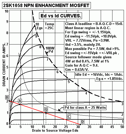
2SK1058 mosfet curves show the dynamic drain resistance Rd for
different
values of Eg-s. Rd then goes over a "knee" and becomes a high
resistance
above Eds = +10V. A model of the mosfet would be a current
generator
producing between 0.3A/V at Id = 0.3A, to about 1.8A/V at 6A, and
the Rd is
a variable shunt resistance above 1k0 at 1A, but reducing to 200r
at 2A, and
less than 80r at 4A. The curves are a guide only, but can be said
to resemble
those for EL34, which has higher Ea and lower Ia ranges. The
mosfet is not
any more linear than an EL34, and in class A both devices can do
the same
job, although the tubes needs a more expensive OPT.
Data sheets for 2SK1058 suggest Pdd, ie, heat produced within the
mosfet
= 100W. This could be be only for a very short time, and curves
show you
could have +16Vds, and Ids = 6.25A, which is 100W. 2 mosfets
easily make
100W Po into 8r0, with Pdd at idle of less than 1W, but operation
is class B.
An EL34 with Ea 400V can make max Ia = 0.3A, an instant Pda =
120W, and
they can make 60W Po in class AB. If such max Pdd of 100W+ are
sustained,
the devices overheat and destroy themselves quickly. Both 2SK1058
and EL34
should NOT have more than 25W of heating for continuous Vdc x Idc
and
or Vac x Iac conditions.
All devices operating in Class A produce heat at idle without any
signal.
The heat is called power dissipation, Pd, and is calculated
Pd = Vdc x Idc = Watts of heat where Vdc is Vd-s, Va-k, Vc-e, Idc
is Amps.
For class A, the idle Pd is constantly high, and device is hotter
than for class
AB amps which may run cool most of the time. The class A amp draws
a
constant power of Vdc x Idc from a PSU, and the AF Po can only
ever be a
maximum of about 45% of the PSU power. The class A devices begin
to cool
as soon as they generate Po. A class mosfet may have idle Pdd =
16W, but
if it makes 7.5W of Po, the heat of the mosfet reduces to 8.5W.
Fig 1B. Testing mosfet for class A properties.
Fig 1B shows an N type power mosfet in class A circuit where Id
> 0.3Adc.
The schematic shows a large effort is needed to find out the
working
characteristics and to measure Vo and THD and draw a graph for Vo
vs THD.
(((For P type mosfets, the PSU and el-caps must be re-arranged for
a
negative B- supply.)))
Input Vac should be 1kHz sine wave with THD < 0.01% from signal
gene with
Ro < 600r.
The gate has a fixed Vdc bias derived from C6 shunted by 4.7V
zener diode
fed from B+ via R8 2k2.
The Idc current can be controlled by change of VR1, using
multiples of
47r x 5W resistors soldered in until the wanted Idc can be
measured across
R5 1r0.
The Ed-s can be controlled by altering the output resistance of
the B+ supply
by change of VR2, shown as 10r0. Rout of PSU = Rw of PT + diode R
+ Rw L1
+ any other R such as VR2. If all this totals 12r0, then Idc
change from 0.3Adc
to 2Adc should cause B+ to reduce from +39Vdc to 19Vdc. This tends
to
prevent excessively high Ed-s and excessive Pdd of mosfet; Pdd =
Ed-s x Idc.
If Pdd is 25W for any test, then max Po may be about 11W for RL
between
8r0 and 40r, so max VRL is between 9.0Vrms and 21.0Vrms.
At 1W, expect THD > 0.1%.
Choke L1 is needed to keep drain Vdc close B+ but give a high Z
drain load.
The Hammond 193u may be suitable, data says is OK for 2Adc, L =
0.2H
and Rw = 1r7. No other data is given for Fsat, Vac with Idc, Bac
or Bdc.
L1 choke could be made as follows :-
Core = T32mm x S64mm x H16mm x L48mm, GOSS, with air gap adjusted
for max L at 2Adc.
Wire = 360turns, 1.12mm Cu dia, 1.217mm oa dia, 10 layers at 36t
per layer
with 0.05mm insulation between layers. Rw = 1.56r, so max heat at
2Adc =
6.24W, OK because the choke has a big enough surface area to
radiate that
heat. With gap adjusted for Bdc = 0.6Tesla, the Bac may be
0.6Tesla with
Vac = 24Vrms at 12.2Hz, for total Bac+Bdc = 1.2Tesla.
The max L1 = 0.22H at about 30Hz, and expect ZL at 1kHz =
350r.
XL1 is in parallel with RL. If RL = 40r, the total Z R//L =
39.74r, so the L1
gives negligible change of RL ohms or phase shift so the L1 has
very little
effect on measurements for Vo, gain, Rout, THD, Po for 1kHz.
For higher L, use a big core with T51mm x S51mm++, taken from any
old E&I
lam PT. Cut off all wire and bobbin, use knife to peel off lams to
get all E and all I
into two separate stacks. Make a bobbin with 2mm fibreglass sheet.
Wind on
52t 1.25mm Cu dia wire on each of 13 layers with 0.1mm insulation
between layers.
Total turns = 676. Average TL 51mm stack, Rw =2r6. With 2Adc, set
gap for max
L which should be 0.52H, and µe should be = 100 for Bdc =
0.6Tesla. XL at 1kHz
= 3k2, and max VL can be 47Vrms at 15Hz with Idc = 2Adc. For more
info on
choke design, try my choke
design pages.
Without any RL, the drain RL of mosfet = inductance of L1 shunted
by R6
which tends to keep Vdc at Vo after C5 15,000uF close to 0V when
no RL
is connected. If the mosfet gm is 0.6A/V, gain could theoretically
be gm x XL
= 0.6 x 350r = 210.
If a CCS was used instead of L1, then RL = R5 100k and gain =
60,000,
which seems quite impossible, but the horizontal Rd lines for Id =
1A indicate
gain is infinite where RL is infinite, ie a horizontal loadline.
A practical CCS could be similar to Fig 5 below so that CCS has
very high
finite R above 100Hz but has very low R at dc, because the CCS
mosfet
elements are source followers which have gates referenced to a
fixed Vdc
with R divider network. Gate of CCS is driven with C from below a
source
R, and the circuit has stable Vdc. The Fig 1B would need to have
B+ at say
+70Vdc if there was another power mosfet as CCS between B+ and
drain
of mosfet being tested. In this case, the choke is adequate as a
high Z load
for ac, but a low Z load for dc, and wastes less heat.
For all RL below 40r, the gain of Vd-s / Vg-s is very close to gm
x RL, and
not affected by any equivalent internal resistance between drain
and source.
There are internal capacitances between all 3 electrodes of
mosfets which
affect the measurements above 20kHz. For example, IRFP240 has Cg-s
= 500pF, with Cd-g = 160pF, and at 1kHz, Xc 160pF = 1M. But if
gain
= 1,000, the Miller C = 1k0, and is in series with 600r of signal
gene, so just
what the gain without any load is a mystery to me. The Rout of
power
mosfets can be considered much higher than any RL connected, and
the
theoretical DF = RL / Rd = RL / infinity = 0.0, a crazy result.
With mosfets, we may never know the Rd value, and certainly not by
gazing
at data curves, and a Google search reveals incomprehensible BS,
and many
things not needed to be fully understood. But Rd is always much
higher than
any likely RL we might use in an audio amp. As soon and any
external loop
NFB is used, effective Rd, ie, the apparent equivalent R between
drain and
source becomes easy to calculate as Rd eff = 1 / ( ß x gm ).
If gm = 0.6A/V, with source follower connection Rd = 1 ( 1 x 0.6 )
= 1.66r.
SF connection has all the Vo is fed back in series with Vin, so ß
= 1.0.
If Rout from source to 0V is measured, it is 1.66r.
If ß was say 0.2 with a shunt NFB resistance network, the
effective Rd =
1 / ( 0.2 x 0.6 ) = 8.3r. If the load on that mosfet is say 16r,
then the
DF = 16r / 8.3r = 1.92, so a little NFB goes a long way to reduce
Rd,
and with ß only 0.2, the Rd curves would appear to have slopes of
8r3 and
much steeper than for common source connection as I have in Fig
1B.
Radiotron Designer's Handbook 1955, page 393 shows where the
Ea vs Ia curves for a typical beam tetrode are shown with similar
Ra shape
to Rd in Fig 1A above. Over laid on Fig 7.88 on page 393 are the
Ra curves
for the same tetrode connected as a cathode follower. The general
ideas of
RDH4 can be applied to mosfets. Following pages in RDH4 give very
fine
graphic explanations of the change of device internal resistance
with applied
NFB.
Vripple at C8 22,000uF at 2Adc = 0.2Vrms. With VR2 = 10r0, Vr at
C7
22,000uF = 1.5mV, so hum from PSU should not upset any test
results.
Fig 1C. Class A, 2SK1058.
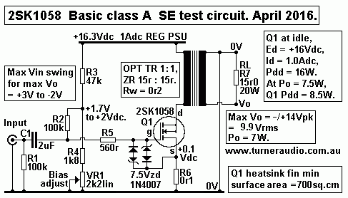
Fig 1C shows a 2SK1058 set up to make an extremely simple 7W amp
with operating conditions depicted in Fig 1A. The single 2SK1058
has an
OPT to couple to an output load. The OPT has ratio TR 1:1 and ZR =
1:1,
and with 15r0 at output sec winding the mosfet drain RLd = 15r0.
Rw may
be neglected. The idle bias current is set by VR1. In practice, at
turn on, the
mosfet is cold and will take time to warm up. If Id is set at 1Adc
when cold,
Idc will reduce as mosfet warms, this is the action of "negative
temperature
coefficient". The bias is re-adjusted as the device warms over
30minutes
until a point of equilibrium is reached, and the mosfet and its
heatsink should
feel warm to touch, but not scorching hot.
The single 2SK1058 has Ed = 16Vdc, and Id = 1Adc, Pdd = 16W at
idle.
The drain is fed from the +16.3Vdc rail via transformer inductance
with low Rw.
The mosfet is like a resistance = V / I = 16Vdc / 1Adc = 16r0.
Although this is
true, the "drain resistance", Rd, which is the dynamic resistance
looking into
drain is much higher, and shown by the Rd line for Eg-s = +2V on
data sheets.
This Rd line at 2A appears horizontal, so that Rd is infinite
ohms, but will be
a finite number of ohms above 1k0. Rd can be measured if the drain
voltage
was forcibly changed by a low impedance voltage source connected
across
RL, while Idc condition Eg-s is kept constant. So Q1 is definitely
STRANGE,
because it acts like a plain old R but also acts like a very high
R.
The presence of R6 = 0r1 is to measure Idc and Iac flow in the
mosfet.
R6 has such a low resistance that it has negligible effect on the
operation
but does offer very slight current NFB to the dc and ac operation.
Class A operation is defined by the active device changing peak
signal load
current by equal amounts for +/- Vpk swings. The Ipk +swings
cannot be more
than the idle dc current in the active device. There is only one
RL value which
allows the highest possible +/- Ipk change = idle Idc, and gives
the highest
possible class A Po.
Fig 1A shows "Rd diode line" below 4A to 0.0A having resistance =
Ed/Id
= 2V / 4A = 0r0.
All mosfets working in class A will involve max Id pk > 4A.
The load for max class A Po may be calculated :-
RLd = Ed / Id - ( 2 x Rdiode ) ohms.
This case, Q1, Fig 1B, RLd = 16V / 1A - ( 2 x 0.5 ) = 16r0 - 1r0 =
15r0.
The max class A Po = 0.5 x Id dc squared x RLd for max Po W.
This case, max class A Po = 0.5 x 1.0 x 1.0 x 15 = 7.5W.
OR max Po = Vd rms squared / RL = 10.6Vrms x 10.6Vrms / 15r0 =
7.5W.
OR max Po = IRL rms squared x RL = 0.7071A x 0.7071A x 15r0 =
7.5W.
While producing class A Po, power drawn from PSU output is
constant,
with constant Idc and Vdc.
When any class A Po is produced in any RL, the Pd in class A
devices
= ( PSU Po ) - ( Po RL ), = 16W - 7.5W = 8.5W. At max class A
Po,The ac
current is the same in RL and mosfet, 0.7071Arms. We might
conclude that
during class A the mosfet acts has R where Pdd = Irms squared x R.
So R = Pdd / Irms squared = 8.5 / ( 0.7071 x 0.7071 ) = 17r0.
There is no need to know this irrelevant information because the
device
is not equal to a 17r0 resistance. The mosfet is a voltage
controlled current
source with very high internal resistance Rd.
At lower Po levels < max Po there is is a dc component. I leave
those with
clearer minds and better at maths to confuse us all, but all you
need to know
is that while class A Po is produced, the mosfet or other device
has lower Pd.
With RL say 5r0, max RLpk = idle Idc = 1A = 0.7071Arms and max
class A
Po = 2.5W. The mosfet Pdd reduces from 16W to 13.5W.
Fig 1A curves for 2SK1058 were scanned from Hitachi's now old
published
data sheets. I have tidied up the curves using MS-Paint. Most
power mosfet
data sheets with Rd curves show very little detail for drain
current < 2Amps.
There is not one single data sheet for any power mosfet which
deals with
class A operation.
Anyone is free to try other types of power mosfets but they need
to think
very carefully about the temperature coefficient and bias
stabilization.
I think 2SK1058 npn or 2SJ162 pnp curves are good enough at below
2Amps
may be more linear than many others with much higher gm and
current ratings.
Fig 1A shows my Pdd curve for 25W, what I consider the safe
continuous
Pdd, something Hitachi and many other makers are too embarrassed
to
include. 25W in a TO3 or TO3P package is enough to raise the
temperature
by +20C where the area of heatsink metal = 40 sq.cm per Watt, ie,
1,000
sq.cm, which would be a single 3mm thick aluminium plate 220mm x
220mm,
mounted vertically, with clear air flow each side. Or else a
finned heats sink
such as Jaycar Cat No HH-8456, with Ahs = 1,050 sq.cm. It has
rating
0.552C/W, so 25W cause 13.8C rise in T; if room T = 30C, heat sink
= 43.8C, and will feel hot if you touch it. The temp inside the
mosfet will be
higher. For 2 x SE or PP mosfets, Ahs = 2,000 sq.cm, for 4 x
mosfets,
Ahs = 4,000 sq.cm. At Pdd = 16W for 1 x 2SK1058, the T rise will
be 9C,
and the Jaycar heatsink would be OK.
Two mosfets for PP action can be used in complementary Series Pair
with
2SK1058 + 2SJ162, with +/-16V rails, Id = 1Adc and total Pdd at
idle = 32W.
The max class A Po = 15W into 7r5. Data curves for 2SJ162 and
2SK1058
show broad similarities but the differences do not allow perfect
complementary
action to cancel all even number HD. However the big reduction of
2H in first
8W is welcome. THD will be mainly 3H, and other odd H. Even with
source
follower connection which is a high amount of series voltage NFB,
at max Po
the THD will be 1%. But at 1W the THD < 0.3% and there is no
crossover
distortion.
In practical circuits, there should be a series source resistance
Rs = 0r47
5W to help regulate the idle Idc, and then must be included in all
calculations.
If an OPT is used, there will be dc flow in windings which may
have Rw of 0r5,
so some Po is wasted. For parallel mosfets, the 0r47 equalizes Idc
and and Iac
and makes each mosfet share the loading equally. Although
theoretical maximum
class A efficiency is 50%, real world efficiency of class A is
rarely ever more
than 45%. From Fig 1A, from 16W DC power input, there is 7.5W
output, so
efficiency = 100% x 7.5W / 16W = 46.8%. If Rs = 0r47, Eff = 45%.
If the OPT
has Rw losses of 7%, then Po = 6.7W, so Eff = 42%. It is no use
worrying
about such losses, and if you don't like losses, use more mosfets.
Fig 2. 2SK1058, SE class A, load line RL 40r.
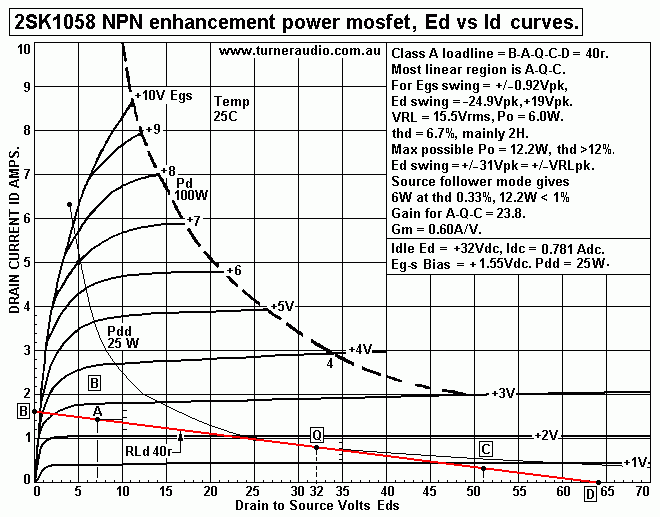
Fig 2 shows 2SK1058 has idle Pdd = 25Watts at +32Vdc x 0.781A.
With RLd = 40r, Gain = 23.8x, and THD seems to be higher than for
15r0
in Fig 1A. But the source follower mode reduces gain to 0.96, thd
is reduced
by same factor 1 / ( 23.8 + 1) , x 0.0403, so expect 6W at 0.27%
and 12.2W
at 0.5%, a better result than for 15r0 in Fig 1A.
A PP pair of N and P mosfets in series will produce less THD
during first 6W
because most 2H cancels. Load = 20r for class A, max Po = 24.4W.
4 PP mosfets give 49.8W to 10r0, 6 give 73.2W 6r6, and 8 give
97.6W to 5r0.
The PSU has to make 50W of power per pair of mosfets for class A,
so with
9 mosfets the PSU makes 200W, and that requires a gigantic
heatsink with Ahs
= 8,000 sq.cm.
Once you have 2 mosfets in PP, the action may be allowed to be
class AB
with idle Pdd per mosfet at say 13W with idle Idc = 0.4A, which
gives the same
max Po = 12.3W into 20r, but the pure class is reduced to 6.4W,
probably plenty
for most ppl, and for 4 mosfets class A = 12.8W with AB ceiling of
49W,
and PSU needing to make 52W.
8 mosfets have class A = 25.6W, with AB ceiling of 97W, but PSU
makes 104W.
In my 50W
monoblocs I have Ed at idle = +32Vdc, Id = 0.78Adc,
and 4
mosfets, all 2SK134, now an old type, but very good. The 4 are
coupled to a
OPT primary load with with P:S ratio 35r : 5r0, and just like
using 4 x EL34 with
OPT and B+ to a CT on primary winding. This means the 2H
cancelling is very
good, and nobody has ever found the sound any worse than any tube
amp.
I found 2SK1058, 2SJ162, 2Sk134, 2SJ176 to all have good thermal
stability in
class A where the device will operate at perhaps 50C with the heat
sink at 40C.
The characteristic data curve sheets show a positive thermal
coefficient below
0.2A, where it is neutral, then negative coefficient above 0.2A.
Best class A use
demands idle Id > 0.5Adc, but 0.4Adc is OK for multiple
mosfets.
For all these Hitachi mosfets, the bias setting for SE or PP amps
requires a
patient mind because after initial setting of Idc of say 0.75A
when cold, the
mosfets warm up, and Idc reduces, and the biasing will take about
30 minutes
before an equilibrium is reached where Idc becomes constant when
heatsink
has reached a stable temperature of say 40C, or 20C above room
temperature.
If the devices work hard in class A, they cool slightly, so Idc
increases slightly.
If they work in AB the Idc increases so they warm up, which
reduces the Idc.
They have very user friendly character, and I have had no mosfets
ever suffer
thermal runaway. There is no need for active bias control which
reacts to the
temperature of the mosfet cases.
SS devices fail much faster than any vacuum tube and you have not
got much
time to measure around the circuit to assess the operation before
there is a
cloud of smoke or loud bang with bits flying across the room, or
straight into
your eyes, with fuse only blowing after serious damage has
occurred.
You should always use a 40W light bulb in series with the mains at
initial turn
on so if something shorts in the amp, the bulb turns on and 240Vac
mains power
draw cannot exceed 40W with only 60mA in the bulb. A variac is
also helpful
in series to SLOWLY raise the mains voltage after initial turn on
to gradually
raise the B+ and B- so that you get time to detect the currents in
your circuit,
and record them in your notebook, and work out if all is well with
rapid accurate
calculations with your pocket calculator.
In an earlier page on this subject, I included ED vs Id curves and
use for
IRFP240, but after realizing how bad their positive temp
coefficient is, I see no
point in promoting their use by saying how they'd be better than
say 2SK1058.
Fig 3 Ed vs Id curves for IRFP240 with a class A load line is now
deleted.
Here is the useful buffer stage schematic I made :-
Fig 3. Mosfet buffer.
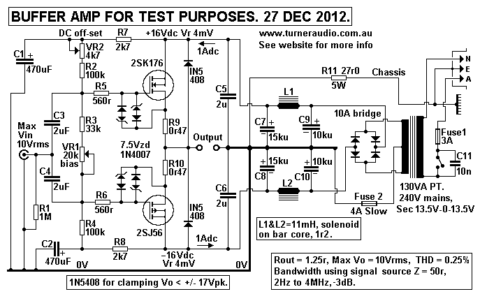
Fig 3 shows old fashioned 2SK176+2SJ56 TO3 devices but you can use
TO3P flat pack 2SK1058+2SJ162, or TO247 flat pack IRFP240+IRFP9240
which can be more simply bolted to a flat surface of a heatsink
that does
not have the flange required for TO3 mounting with two bolts, and
flange
holes for gate and source connections.
The buffer circuit has total Pdd = 32W. For T rise > 20C, the
total exposed
surface area of aluminium fins, both sides, and base plate should
be
40sq.cm per W. Most sold at electronics stores like Jaycar are
barely
large enough for many projects.
The best place I know in Australia to buy a heatsink is from
http://www.conradheatsinks.com/welcome.htm
Heat sinks are difficult for DIYers to design because of the maths
involved.
Inevitably, many end up trying to use a heatsink without enough
surface area
and they install it in a box with poor ventilation. Fans help, but
I hate the noise.
More about heatsinks at bottom of this page.
The properties of the buffer stage:-
Input Z = 45k in parallel to effective gate-source capacitance,
about 150pF
in this case. All signal generators will drive the buffer, and
widest input
bandwidth is possible where signal gene has Rout = 50r.
Maximum Vin = nominally 10Vrms, +/-14pk, but could be slightly
higher
than +/-16Vdc rails to get Maximum Vo = +/-15Vpk = 10.6Vrms, sine
wave.
For Vo = +/-14Vpk, 10Vrms, the load for maximum pure class A =
7r0.
All loads below 7r0 will produce lower levels of Class A Po at low
THD, but
higher max Po levels in class AB with higher THD.
In other words, all load Z above 8r0 can be driven with class A PP
operation
and max class A THD < 2%. But loads of say 100r can be used and
at max
Po the max THD is much less than 2%.
Output impedance < 1r0, shunted with C < 50pF,
Output bandwidth, 0.8Hz to 5MHz, -3dB poles. The HF pole depends
on
low Z input feed source.
Applications, The buffer can be used to lower the impedance of any
signal source to less than 1r0, and can be useful for testing
transformers
for speaker value Z values and for for speaker testing.
Verification. I tested the buffer with 470kHz square waves,
8Vpk-pk. Rise
time is over 50V/uS and the CRO showed that highest F present in
sig gene
wave is about 3MHz. The CRO showed no change of buffer output wave
shape.
Input C of the buffer is slightly variable depending on the output
RL
impedance. C loading at output reduces gain and increases buffer C
in,
thus lowering Zin. Therefore signal gene Rout to buffer ideally
should be
50r to get best HF response. Buffer Cin is lowest where output
load Z
> 8r0, including all transformer or LC or CL networks.
Lower Vo levels down to less than 1Vrms are often quite effective
to
test many loads so the ZL could be 2r0 and the buffer will still
work
in class A because its Rout = 1r0.
For example, consider RL 2r7 bypassed with 50mH. The network has
Z = 1r9 at 8.5Hz, and 1r0 at 4Hz. The buffer response will be -6dB
at 4Hz.
If we wish to know the Z of R//L, we could connect 10r0 between
buffer
and 2r7//50mH, and measure Vac across 10r0, and Vo at ZR//L and
calculate the loading. L+C and C+L speaker filter networks may
have very
low Z at the Xover F, and thus need to have R connected across the
speaker to damp the L+C to make the load become resistive, or
damped,
so an amp does not have work with a low resonant load.
At HF, if RL is a pure 2uF C, the buffer will give a F2 -3dB
response to
79kHz, when Xc = 1r0. But at 800kHz, the pure C load cannot be
more than
0.2uF and at 4MHz not more than 0.039uF.
In other words, the purpose of any test and effects of loading are
kept
in mind at all times.
Hence I found myself using pocket calculators so often the numbers
disappeared from the buttons!
The buffer schematic led me to develop it into a useful amp for
better
educated and practical DIY audiophiles who may not struggle too
hard to
make it themselves, and give them the chance to find if wide
bandwidth and
low THD from class A mosfets gave sound just as good as their much
loved
SE 300B amps or other class A tube amps.
Here is what I think might sound better than a couple of 300Bs in
parallel....
Fig 4. Hybrid - 1A, Amp.
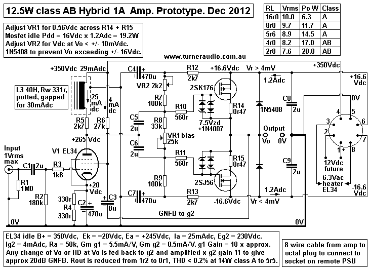
Fig 4 amp is an experimental prototype with a remote power supply
in Fig 10 further down this page, and The amp does exist, see Fig
15 picture
at the bottom of this page.
Fig 4 is a class A PP amp with as few devices as possible - only 3
!
Most characteristics of the amp are typed on the schematic. The
basic concept
is as simple as I could think of, seldom seen anywhere else on the
Internet, so
it needs some explanation of the properties of EL34 behavior and
in this
application. I show mosfet Idle current 1.2Adc and +/-16.6Vdc
rails. There is
0.56Vdc across each R14+R15, so to get the full Ed = 16Vdc, the
Vdc rails
must be slightly higher.
2SK1058 + 2SJ62 may be used instead of 2SK134+2SJ56, with very
little
change to the biasing.
IRFP240 + IRFP9240 may possibly be used, but their positive temp
coefficient
is a major worry, and Eg-s biasing would be +/- 4.2Vdc, so biasing
is changed.
I would not uses these and I don't like having additional circuit
parts to control
bias current.
Any loads above 3r0 may be used. The initial class A power is
enough to cover
most listening with average speakers needing 1W to make 88dB SPL
at 1M.
With 2r8, class A Po = 8.1W, with max AB = 20W. The PSU must have
very low
output resistance, and much better than I used for the prototype.
The PSU rails sag a bit with increased Idc for high Po to a low
Output RL.
Hitachi mosfets have a nominally negative temp coefficient, ie,
they conduct
LESS current if T rises, so fixed bias can safely be used
especially where
source resistors R14+R15 0r47 are used for a small amount of local
current
NFB.
I have also seen mosfets develop queer behaviour faults from
severe overheating,
thus become partially failed, and create strange HF oscillations.
So make sure
you use 0.47r, non inductive types, and at least 5W.
Hitachi gate bias = +/- 2.2Vdc approx. Vdc between both gates =
5.5Vdc approx
with 1.2Adc in R14+R15. VR1 is used to adjust the gate Ed-s bias
for 0.56Vdc
across each of R14 + R15. After this is set with amp well warmed
up, there will
be some +/- Vdc offset at Vo, and VR2 is adjusted to give Vdc
between Vo and 0V
> +/-10mVdc. Once the bias is set, VR1 and VR2 should be near a
center position.
If not, adjust fixed value R7, R8, R9 to achieve this, so that in
future there will always
be enough turn of pot to bias the amp correctly.
With bias set when amp is fully warmed, the bias should not drift
and any Vdc offset
when the amp is cold will not cause enough Idc in a speaker to
ever cause damage
or spoil the sound.
I do not show a protection circuit, but this amp like all others
should have one which
detects Vdc at Vo when it exceeds 1.0V for longer than 3 seconds,
and turns off the
amp. If you have 16Vdc feeding 5.6 ohm voice coil via a shorted
mosfet, the coil has
45W of dc heating, and it is badly damaged after 10 seconds.
The EL34 is set up with L3 choke feed of DC from B+ supply plus
series R5 2k7.
The L3 choke of 40Henry was from my collection of ancient chokes
so I don't know
exact specs, but it has E+I core of unknown iron, probably not
GOSS, but has
Stack = 22mm x Tongue = 22mm approx. Rw = 330r so those winding
their own
would might use Stack 25mm x Tongue 25mm, and just fill the bobbin
with 0.2mm
Cu dia wire. Then an air gap is determined by testing for maximum
L with 30mA dc
present. Probably this is way beyond many ppl's technical ability,
OK, they might
BUY suitable chokes from stores online. But most don't have the
high L needed
and don't have ideal gap size, and you may need 2 in series for
the wanted L.
The 2k7 isolates the effects of shunt C and shunt L in the choke.
The 2k7 widens
the total bandwidth while offering a shelved gain reduction at
below 30Hz and above
10kHz which reduces gain and NFB effects outside the AF band while
reducing
phase shift. This gain shelving is very benign, and always
favourable if any NFB
is used, and much increases the amplifier's margin of stability.
Without L3, and with only R between B+ and anode, RLdc = 2k9, and
the gain due
to g1 grid is much lower, and the gain due to g2 is reduced from
up to about 15
max to less than 2 so that the use of screen g2 input becomes
useless as a NFB
input port.
L3 40H may have XL = 50k at 200Hz, and this is parallel to pentode
Ra of 50k, so
g2 gain = gm g2 x 50k//50k = 0.5 x 25k = 12.5.
In Fig 4 the screen is used as an input port for NFB, and for this
form of NFB to
be worth using the the anode load must be high as possible.
Instead of using a choke plus R between anode and B+, one might
use a CCS.
Fig 5. CCS.
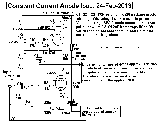
Fig 6 shows a pair of 2SK1924 mosfets in series instead of 2k7 +
40H Choke.
The 2SK1924 are now obsolete, but are TO220 types OK for Vd-s up
to 700V.
They don't like high current with high Vd-s, but here I have
reduced the max possible
Vd-s to about 200Vdc, 1/2 B+of +400Vdc, if EL34 ever becomes a
short circuit.
Other suitable TO220 package mosfets with Vgs rating over 500V can
be used.
The screen g2 gain is about +4dB higher than using 2k7+40H. So
hence the FB is
more effective at reducing the amp Rout and THD. The CCS does
become a
low Z at LF due the R&C network R6,7,8,9,10,11, and C4+C5. But
the CCS finite
resistance remains high to a lower F than a 40H will give. The CCS
does not
introduce iron caused distortions. The CCS has low shunt C at HF.
The CCS acts as a source follower at 0Hz with R12 1k0 between Q2
source
and EL34 anode. The source follower has fixed bias from R divider
from B+ to
0V using R6+7 and R8+9. The C5 2uF bootstraps the divider network
load from
low Z output of Q2 source while C4 keeps the gate shunted by low
2uF Xc
between gate and EL34, so the current in Q2 is kept very nearly
constant.
Q1 has the same constant current as Q2, and is a slave to Q2.
Traditionalists will avoid this solid state buffoonery, and go for
a choke. But
I have used this CCS in other amps which sounded magnificent. The
CCS
is a slave to EL34 which sings better because of the CCS.
Making a 40H+ choke is fairly easy, and does not need neatly
layered windings
but can be wound with polyester-imide coated grade 2 wire with
slow traverse
speed across the bobbin width to avoid wire crossing at high
angles. In many
ancient radios before permanent magnets were available, after WW2,
thousands
of speaker field coils were "random wound" with thousands of turns
of wire with
old fashioned fragile enamel coating, and many still work just
fine.
Operation of EL34 to drive output mosfets may be difficult to
understand.
But don't expect answers elsewhere online. I need to explain basic
issues
and build up from there.
Fig 6. Basic voltage and current generator models.
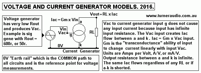
Fig 6 tells us about TWO basic building blocks of electronics.
The voltage generator is any signal source between two points
which has
zero ohms resistance between the points. This is impossible in the
real
world but that does not prevent us considering the voltage
generator then
adding a series R to be equivalent to the the resistance we know
exists
between two points. So a common signal generator or function
generator
will have a known Rout, usually 600r, or 50r and signal level
output is not
altered much by connection to a following load > 100k. In Fig
6, the gene
is connected to a input of a current generator, which could be a
tube grid
or fet gate, or other high Z input.
The voltage gene here has 2 terminals, with one for Vo out, and
other to
0V. The voltage source could be a floating transformer winding
output.
Signal generators don't always have a pair of floating outputs,
and usually
have one output terminal with other always to 0V, because of the
circuit
connection to a mains power supply.
The current generator is usually a three terminal device we want
to use,
bjt, j-fet, mosfet or vacuum tube.
Fig 6 shows a vacuum tube with 3 terminals grid g, anode a, and
cathode k.
The perfect current source has infinite Rin to between g and k,
and infinite
Rout between a and k.
The Vac applied across g and k cause current to be generated
between a and k.
The current change for each Volt of Vg-k change is the generator
"transconductance", aka known as Gm, or gm, and is in units of
Amps
per Volt, or mA per Volt, (or Siemens in SS data sheets.)
There are no perfect current generators because all have some R,
L, and C
quantities between terminals. But for LF the C and L may be
ignored. The Rin
between g and k is usually very high, > 1M0, for gates and
control grids of
fets and tubes. Bjts have low Rin between base and emitter, so
this must be
considered when modeling a schematic.
All current generators have some finite resistance Ro between a
and k.
But if there is a known but high Ro we may ignore its presence if
an RL is 1/100
of the value the Ro, and ignore Ro, ie, consider the device is
perfect.
But for most device models there must be an added shunt R between
a and k
to mimic the effects of a known resistance. In tubes the added
shunt R is Ra,
in bjt its Rc, and in fets it is Rd.
I hope this all liberates your mind about models and devices.
Fig 7. EL34 Gm controlled Iac generator.
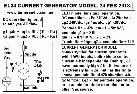
Fig 7 shows an EL34 used as a driver tube for amp in Fig 4 and Fig
5.
EL34 has 5 active electrodes, cathode at its centre, emitting
electrons
in a cloud, then a control grid g1, then screen grid g2, and
suppressor
grid g3, all concentrically arranged with anode being outermost
electrode,
the dark grey "box" we see through the glass. More info about
basic tube
behaviour is in my pages starting at
http://www.turneraudio.com.au/basic-tube-1.html
g1 and g2 both have some control the flow of electrons from
cathode to
anode. The tube may be modeled as a pair of current generators
each as
shown in Fig 6, but can be shown in Fig 7 as one current generator
with two
inputs, with each input controlling the one electron flow
independently.
At the DC idle conditions given, EL34 pentode Ra = 42k. I measured
gm g1
= 5mA/V, and gm g2 = 0.5mA/V and measured Ra, and my figures are
very
much different to what data sheets show based on much higher Iadc.
For all tubes, µ = Gm x Ra.
This works for where you know what Ra is and what µ is for a given
input
grid and the anode-cathode Va-k, also = V RL. With real triodes
and
pentodes strapped as triodes, the Ra is often conveniently low and
predictable.
For RL = CCS for EL34, ie, RL > 1M0, ug1 = 0.005 x 42,000 =
210.
The g1 gain with CCS RL = µ where g2 is held at constant V between
g2 and k.
For g2 operation with Vg1 = 0V, and signal current controlled by
g2,
Ra is the same as for pentode = 42k, so with CCS anode load µg2 =
0.0005 x 42,000 = 21.
Where g2 is connected to anode for triode operation, Va is applied
to
g2 so that g2 generates current = g2 gm x Va. The resistance
between
a and k is Triode Ra, and calculated as Va / ( Va x gm g2 ) plus
parallel
pentode Ra.
This is more simply Ra = ( 1 / gm g2 ) // pentode Ra.
Triode Ra = ( 1 / 0.005 ) // 42,000 = 2,000 // 42,000 = 1k9.
The 1k9 is much higher than data sheets giving EL34 Ra = 1k25.
But it is quite low enough for use as a small signal amp in.
My figures are OK for pentode and triode Ra and about correct if
you
can read the bottom part of the old data curves for Ea vs Ia Ra
for the
EL34.
The bottom part of curve sheets is where most of the amplifier
action
occurs, but where the data sheets are most inaccurate.
Fig 8A. EL34 pentode, RL 3k3.
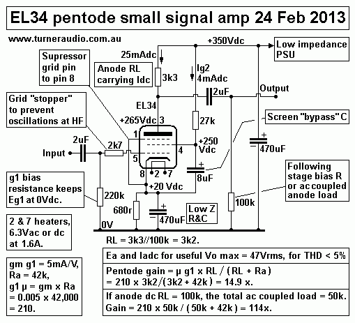
Fig 8A shows an EL34 in pentode mode for a small signal voltage
amp.
I have an EL34 driving anode dc carrying load of 3k3 // 100k for a
gain
14.9x. This is medium gain < 20, and we would find the
bandwidth may
reach 1MHz. The Rout is the 3k3 // Ra 42k // 100k = 2k97. So
although
pentodes have high Ra, their RL is often much less than Ra, so RL
determines the Rout for the stage. With idling 25mAdc, it could
produce
about 50Vrms. But THD would be fairly high because there is no NFB
loop and the tube is not performing in triode mode.
Fig 8B. EL34 triode model.
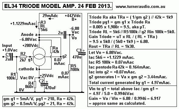
Fig 8B shows how the triode connection can be modelled.
The operating conditions are similar to Fig 8A, with higher RL and
B+.
Ea = Eg2 with g2 connected to anode. Ea is about the minimum for
good
linear operation for the triode. I have RLdc = 5k6 for 25mAdc to
anode
and 4mAdc to g2 screen from +442Vdc B+. The analysis shows
calculation of triode Ra, and the total RLa and the gain of 6.88x.
Also shown are the totals of current change due to a Va change of
6.88Vac
The total of all these Iac must be produced by g1, and the
analysis concludes
that gain calculated from Vac and Iac analysis is the same as the
gain
calculated by simple formula, Gain = µ x RL / ( RL + Ra ).
The screen grid 2 is the most mysterious electrode because so
little is
written about it. Its original function was to interrupt the
effect of electrostatic
field change between anode and cathode, so that the Miller input
capacitance
was hugely reduced allowing bandwidth from DC to many MHz.
Without the anode's electrostatic field change reaching and
summing with
action of g1 grid, the pentode can give much higher gain than when
triode
connected, where gain is never more than triode µ.
Screen g2 draws dc current, and has a finite Rin lower than g1. g2
Rin
= 100k approx, and is a load which the anode must drive.
The suppressor grid 3 in EL34 is not considered in the model
because it has
a minor role of preventing secondary emission, see the relevant
texts on this
elsewhere. EL34 suppressor can be connected to anode or 0V when
tube is
triode connected. But for pentode connection, suppressor pin 1
must be
connected to cathode pin 8 or else you will see a huge amount of
distortion
and queer behaviour.
With EL34 triode strapped, the Va applied to g2 causes an opposite
phase
of signal current to that produced by Vac input to g1.
+1V at g1 produces 5mA increase in anode current, which increases
RL
current so the anode swings -V = triode gain x Vin. The -V at g2
reduces
anode current, and the two g1 and g2 electrodes have opposite
effects
on Ia, with g1 having the greater effect. In real triodes like a
300B without g2,
the anode has the same electrostatic effect on Ia as a g2 screen
in a pentode.
The TWO electrostatic effects by g1 and g2 sum together to give a
net result
which constitutes the action of internal electrostatic shunt FB.
Its the FB which
makes triodes have their desirable character of low Rout and low
THD.
g2 produces gain = µg2 x RL / ( RL + Ra. ) In Fig 8B, RL = 5k0.
µg2 = 21.
Ra = 42k. So if any THD appears at anode, it is applied to g2, and
amplified
by the g2 gain = 21 x 5k0 / ( 5k0 + 42k ) = 2.23x. With -6.88Vac
at anode
for +1Vac to g1, we might expect THD = 0.5%. ( 3.6% at Va = 50Vrms
).
So THD at anode = -0.0344Vac. This is applied to g2 which tries to
make
+0.0776 Vac appear at anode. But we measure -0.0344Vac. So without
g2
having any signal, and for the same Va = -6.88Vac, pentode gain is
23x,
and Vin g1 = 0.3Vac. The pentode THD could be expected to be
higher than
the triode, and probably +0.112Vac. When g2 is strapped to anode,
the
pentode gain reduces from 23 to 6.88, a reduction of 1 / 3.34. So
the THD
produced by pentode is also reduced by the same factor, the triode
THD
= pentode THD - correction signal by g2 = +0.112 - 0.0776 =
+0.034Vac.
The g2 acts as a port for NFB, and THD in triode is usually much
less than
pentode.
With a higher RL value, the g2 gain increases and reduction of
pentode THD
is increased. Maximum linearity is achieved with the RL being a
CCS, or a
high value choke acting to give a high RL value well above the
pentode Ra.
Triode loadlines for high value RL do show magnificent linearity,
with 1%
at 50Vrms being possible.
Consider a CCS with finite Ro = 500k to replace the DC RLa of 5k6.
Resulting load at anode = 500k // R5 100k // 100k of g2 Rin =
45k5.
Pentode gain = 210 x 45k5 / ( 45k5 + 42k ) = 109x
g2 gain = 21 x 45k5 / ( 45k5 + 42k ) = 10.9x.
Triode gain = 9.5 x 45k5 / ( 45k5 + 1k9 ) = 9.12x. The gain
reduction factor
is 1 / 11.95. In other words, where ratio gm g1 : gm g2 = 10 : 1,
expect the
triode connection to try to reduce pentode THD by factor
= 1 / (1 - [ Pentode A / Triode A ] ).
Although triode strapping does give a lot of NFB, the gm g2 for
gain is not
linear just the g1 gm, because Ra varies with Ia. Ia change by
means of
electrostatic field control is subject to a formula where
Ia = K x Vin to power of 2/3, ie, Ia = Constant x cube root of Vin
squared.
The less Ia change there is, the more linear the triode becomes.
In Fig 4 amplifier, g2 is NOT connected to anode, and NOT bypassed
to
cathode, but instead bypassed to the Vo of a mosfet source
follower output
stage. This output stage has gain not much less than 0.9, so the
Vac at EL34
g2 equals 0.8 x anode Va. BUT the THD of the output stage is added
to
the pentode THD and both sources of THD are reduced by the g2 gain
and EL34 acts like a triode, with slightly higher gain because Vg2
is slightly
less than Vg1. So the EL34 Pentode is fooled into behaving like a
triode,
and does a bit of extra work for free!
Fig 9. EL34 model driving source followers.
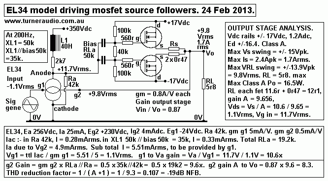
Fig 9 has the equivalent model of the EL34 as used in above Fig 4
schematic to drive a complementary pair of mosfet source
followers.
The mosfet output Vo is placed within the loop for triode
connection.
The mosfet stage gain 0.87, and the EL34 Va = 11.7 Vac max to give
VRL max 9.8Vrms. This is a low Z signal source which drives the
high Z
input of EL34 g2. The total anode load of EL34 is reactance XL1
50k
parallel with to bias R load, 50k, which totals 35k at 200Hz. g2
gm has to
power the 35k plus parallel Ra 42k for total of 19.2k, and g2 gain
= 9.6.
The g2 to gain to amp Vo = 9.6 x 0.87 = 8.3. If measured THD at Vo
= +0.02Vac, it is amplified to make a correction signal -0.166Vac
at Vo,
so THD without FB must have been +0.186V, so THD reduction factor
= 0.1075.
THD reduction factor = 1 / ( A + 1 ) where A is the open loop gain
between
Vo and a point in voltage gain amp for NFB. Gain is regarded as a
positive
number, but in fact the gain is negative, because g2 produces an
opposite
phase of signal at Vo. If you must consider A negative, then the
formula
must be 1 / ( A - 1 ) and because A is really -A, then RF = 1 / (
-A -1 )
and this simply means the RF = 1 / ( gain number greater by 1.0 )
The XL1 varies with F and at 20Hz its only 5k0. So by 20Hz, the g2
gain has
reduced to maybe 2, so THD reduction is low, and the EL34 works
more like
a pentode and THD is higher. But there is not huge music content
at 20Hz.
At 1kHz, L1 inductance may be 10H, because the iron µ becomes
lower with
rising F. XL1 will be 63k, and the load powered by g2 rises
slightly so g2 gain
increases slightly so the THD reduction is increased.
Obviously, the higher the L1 inductance, the better, and 100H
would be nice.
Best of all is a CCS load for EL34 anode.
The THD reduction calculated is a useful amount. Mosfets rarely
need to
make more than 20Vrms to any speaker load, the EL34 produces much
less
THD than the source follower mosfets. EL34 in triode could give 1%
THD at
100Vrms for a CCS load. The NFB connection with g2 screen reduces
EL34 gain to similar to triode µ of 9.5, and here I calculated
1.1Vrms is needed
at input so sensitivity is convenient for about everyone.
Although the EL34 is a pentode with high Ra, with the NFB giving
similar to
triode operation it easily can power the input C of mosfet gates,
and NFB
action flattens any sag in Vo. The Fig 4 amp HF bandwidth shows
only -2dB
reduction at 200kHz !
For those who still cannot accept GNFB or screen FB or any loop
FB, they
will at least have to accept the local NFB generated in the source
follower
connection, which is an application of "series voltage NFB" and
the same as
used in a cathode follower which meets wide acceptance.
But if screen NFB is omitted, then 6 mosfets may be used with +/-
22Vdc
rails and with each mosfet having Id 0.7A for Pdd = 15W. This
gives total
Pdd at idle = 90W, so a big heatsink at least 300mm long x 200mm
high
with 30 x 40mm fins are needed. But you get a maximum of 35W
pure
class A of class A power for 4r8. You will find little need for
loop NFB at
normal levels where each mosfet works with RL = 29r and where its
open
loop gain, Vs / Vg-s = 20 approx, and THD reduction factor = 1 /
21 = 0.05,
or -26dB. If THD in class A without the follower connection was
10%, we
might expect 0.5% with the follower connection at 35W. At 2W THD
< 0.1%,
some say that's fine.
Other pentodes and beam tetrodes also will work fine as driver /
input
tubes, EL84, EL86, EL36/6CM5, KT88, 6550. All such tubes have
screens
and EL36/6CM5 having highest screen gm of about 1.4mA/V, giving
high
g2 gain if the RLa is kept high.
In my 1999 50W
mosfet amps I use an OPT and have 4 x 2SK134 arranged
in common source mode - just like a quad of EL34 driving an OPT
with CT
and B+.
In these 50W amps I have a simple differential input pair using
bjts to produce
the low signal voltage of about 1Vrms needed to drive mosfets to
clipping
levels. There are two forms of NFB, balanced shunt voltage NFB and
global
series voltage NFB which roughly is the same total amount of NFB
used with
source follower connection NFB to tube g2. The 1999 design
probably would
work better if the mosfets were used in source follower mode and
tubes
were used to produce the higher balanced 42Vrms gate to gate. A
future
project would include the addition of a pair of EL84 in triode
plus an input triode
similar to my existing designs for input driver stages to my 300W
& 8585W
tube amps.
There is nothing wrong with using an OPT with mosfets because it
allows
variable load matching so that one may obtain the same amount of
pure class
A Po with any load between say 2r0 and 16r0.
Power supply for the Simple Hybrid Amp is here....
Fig 10. Hybrid - 1A, PSU
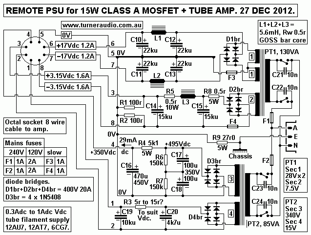
Fig 10 PSU is generic, and as simple as possible. No regulation is
needed.
The +/- 17Vdc rails can vary slightly if the output power becomes
class
AB for a low RL value. L1+L2+L3 chokes are 5.6mH and a bar core
type
with Rw = 0r5 usually used for speaker crossover filters should be
OK.
The effective iron µ will be only about 4, and the Idc will not
saturate the
iron. Air core chokes have too much Rw. With 2Adc, Pd = 2W, and
none
of the chokes should get hot. Keep all chokes and el-caps well
away
from the heatsink and where they get a rising air breeze via holes
in
chassis. Using E&I from a small 10VA power trans and with an
air gap
will increase the iron µ to maybe 100, and much reduce the number
of
turns and reduce the Rw. Extremely keen ppl will read my pages
on choke design.
Fig 10 PSU is also good for the Amp with IST in Fig 12.
Fig 11. Graph Po vs RL.
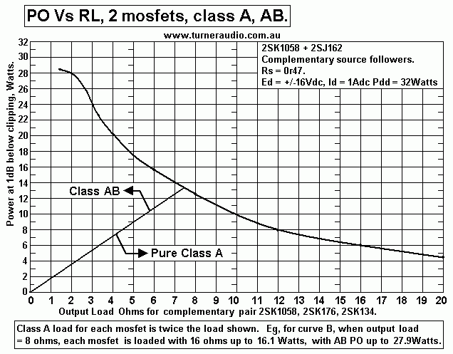
Fig 11 gives Curve A for 2 mosfets and rails at +/- 16Vdc, and
idle
1Adc in both mosfets, with total Pdd being a very mild 16W for
each
mosfet. There is a useful 8W in pure class A for all loads between
4r5
to 12r0.
Max class A Po = 13W for 7r5, approx, max class AB = 28W to 2r0.
The THD is lowest in class A region, and will become high for RL
< 3r0.
The class AB Po depends on regulation of +/- 16Vdc rails while
class A
Po has constant PSU power so the +/- rails don't sag when making
Po.
My prototype had no active regulation of Vdc rails and had CLC
filtering
where the L had Rw 1r2, a little too high.
Fig 10 shows the two C are = 22,000uF, and choke is only 5mH, a
bar
core used in speaker crossovers with Rw 0r5, and with 1.2Adc, the
100Hz
V ripple at CLC output < 3mV.
Fig 10 shows PSU for +/- 17Vdc, and 1.2Adc so Pdd per mosfet =
20W,
and this allows class A Po = 16W into 5r8.
4 mosfets in similar Ed & Id conditions would give more class
A power to
lower RL and higher maximum class A Po.
Instead of a complementary pair of npn and pnp mosfets, a "quasi
complementary pair" may be used with a series pair of N type or a
pair of
P type.
This means the "top" mosfet is in source follower mode with gate
Vac
slightly more than its source output and with same phase. The
"bottom"
mosfet is in common source mode with its RL in its drain circuit.
The bottom gate Vac is much less than at top mosfet gate, and has
opposite
phase. This form of Quasi Comp Pair was the first way used for
early SS amps
before N and P devices could be made with similar properties,
although of
opposite type.
I like to just call the QCP more simply - Series Pair, there isn't
any quasiness
worth considering.
Various methods have evolved to ensure the Vg-s of both mosfets of
bjts remain
the same amplitude under all working conditions so that they
equally contribute to
generating Po.
The Technics driver was a popular method to drive a Series Pair.
EL84, EL34
can be used more easily to drive a Series Pair of mosfets than
trying to drive
a series pair of power triodes like 6C33C.
The Technics driver is a concertina phase inverter aka split load
phase inverter
where the output from Series Pair is used as NFB to make the pair
of mosfets
both work as "followers".
The 1:1 Interstage Transformer is another method of providing
balanced drive to
Series Pair. IST is 5k0 : 5k0 or 10k : 10k. Mass manufacturers
avoided this
because the IST cost more to make and install compared to a single
bjt and a
few R&C. However, the IST is OK for the DIYer who should not
worry over costs.
Fig 12A. Hybrid - 2A, with Interstage Transformer !
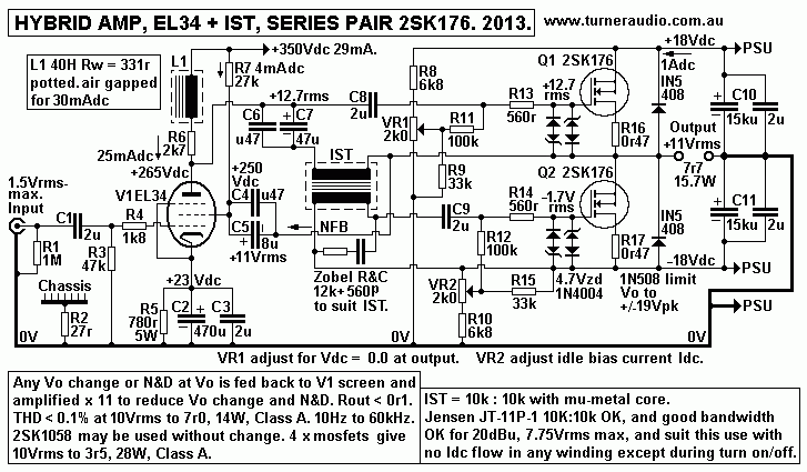
Fig 12A shows the same type NPN mosfet for the Series Pair output
stage.
The Vgs needed for either mosfet for most Po is always less than
about 2Vrms.
EL34 anode drives Q1 gate but between anode and Vo, there is a
capacitor
coupled high Z primary of IST. Therefore Q1 Vgs is across the IST
primary.
The IST secondary has same amplitude Vac, but applied to Q2 Vg-0V
and
with opposite phase.
If Vo changes due to change of output RL, or if any THD is at Vo,
then an
"error" signal is applied across the IST primary, and between Q1 g
and s so
Q1 operates as a source follower. But the same error signal with
opposite
phase is produced at IST sec and applied between Q2 g and s. So Q2
also
works as a follower with the same amount of local NFB as Q1.
The IST has very low Vac compared to normal use in a tube amp. The
IST
can be small and have high bandwidth, and there is no Idc in any
winding so
an air gapped core is not needed.
This IST is arranged and designed so its loading effect on EL34 is
negligible.
The EL34 has all the Vo applied to its g2 for NFB. So any error
signal is reduced
by NFB.
Using identical NPN mosfets attempts to maximize the cancellation
of even
numbered HD products generated in both devices because both have
very
nearly the same transfer curves.
IST may be too much of a challenge for some folks but the
alternative to the
IST is another amp stage with a tube for a "bootstrapped" phase
inverter.
Most DIYers loathe the cost of the IST and they don't know what
sort of IST
to buy. They don't how to wind their own, or where to buy the
cores or wire.
I figured the IST could have 10k : 10k primary to secondary
impedance ratio so
that loading of EL34 anode is negligible. With 10k primary input.
Large IST with
GOSS cores to drive 845 grids with say 120Vrms are not needed, and
here we
need what is really a 10k:10k Line Level 1:1 transformer. The
Jensen JT-11P-1
would most likely be OK.
http://www.jensen-transformers.com/wp-content/uploads/2014/08/jt-11p-1.pdf
The signal specs say level can be 20dBu. Now 0dbu = 0.775Vrms
applied to
600r which generates 1 milli-watt of power, and 20dB above that
means 10 times
the Vac, say 7.75Vrms. In this circuit the Vac across primary is
the difference
between gate and bottom of Rs 0r47. This Vac is highest when RL at
output is
say 3r0, and high levels may give Id pk = 4Apk, and the Vgspk =
4Vpk VRs =
1.9Vpk, giving total 5.9Vpk which will be limited with zener diode
+ diode at this
level.
With RL = 7r0 for class A Po, primary input Vac > 3Vpk at
clipping.
The Jensen has a mu-metal core, µ is high, size fits inside 30mm
dia x 30mm high.
The Rw of P and S are each 1k5, so wire size must be very small
dia, and easily
fused by accidental excess current. Loading of sec winding with
100k should
cause 1.5% imbalance between Vin and Vo, and negligible. I show
12k0 + 560pF
loading of sec so that above 28kHz, the sec load becomes
resistance to prevent
any peaking in response; but this may not be needed.
The 10k:10k nominal impedance means that the primary inductive
reactance
XLp = 10k0 at the -3dB pole, but the Jensen F response shows -3dB
at 0.2Hz, but
that may be with Sig gene with Rout 50r. That implies Lp = 40H,
but if the tranny is
fed by source resistance of 10k, then LF -3dB = 40Hz. But in this
circuit the the
tranny is connected between EL34 anode and low Z output from
mosfets. The Ra
of EL34 is effectively reduced from 40k in pentode mode to about
2k0, so the
transformer may possibly have -3dB pole at 8Hz. The problem with
many lists of
properties of available ready made transformers is that they omit
the details about
inductance and the winding geometry.
Can you trust Jensen? I've never used one, they do have a good
reputation.
If the tranny LP is higher than 40H, then LF pole will be lower
and the LF stability
should remain OK because. Some other brands boasted their Lp for
10k input
was 8H, which could be a problem needing a LF gain shelving
network at LF, like
many other amps I have designed.
Fig 12B. Hybrid - 2B, Technics drive for Series Pair 2SK176
or 2SK1058.
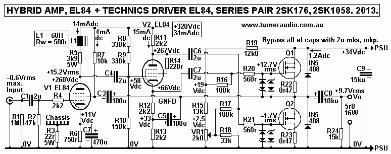
Fig 12B shows the Technics invention of a bootstrapped split load
phase
inverter triode V2 EL84. C5 links amp Vo to bottom of the R12. Iac
and
Idc in R11+R12 are always equal, but output Vac is opposite phase
so
the Vgs for both output mosfets is always the same. V2 cathode
Rout is
less than 150r, so any change of Vo or THD is across R12, thus
changing
current, and the same change occurs in R11, but opposite phase, so
the
bootstrap connection is a form of local NFB to make both mosfets
act as
source followers.
Fig 13. Hybrid - 3, SHEET 1 amp. ( if .gif size too small,
open in separate window )
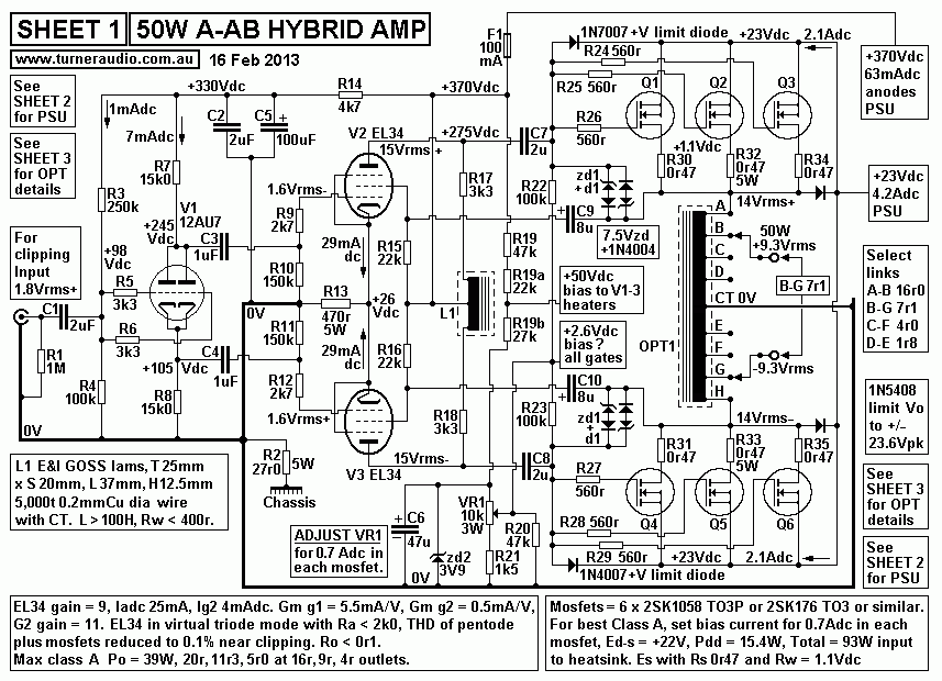
There should be benefits for the greater complexity.
With 6 x 2SK1058 or 2SK176, max total Pdd could be 25W x 6 = 150W,
and possible max class A Po could be about 64W. But the heatsink
size
begins to be too big, and just who needs 64W in pure class A?
Nobody
I know, when they rarely ever need more than 16W of total peak Po
for
each of 2 channels.
Therefore I show the above amp with each mosfet at Ed = 22Vdc,
Id = 0.7Adc, giving Pdd = 15.4W, for a total of 92.4W at heatsink.
Max
class A Po can be about 40W, enough. This much class A Po depends
on
the RL at each mosfet = 29r, and not including 0r47 at source. The
max
Id swing = +/-0.7A so max class A Po per mosfet = 7.105W, so the
six mosfets should make 42.6W class A.
Max Ed swing = +/-20.3Vpk, so Vin across A to H on PP auto OPT =
+/- 40.6Vpk = 28.7Vrms, RL input between A and H = V squared / Po
= 28.7 x 28.7 / 42.6 = 19.3r. These theoretical figures depend on
enough
NFB to make the mosfets produce THD < 0.5%. Idc could be
increased
to 0.75Adc, and B+ supply to +24Vdc, giving total Pdd = 104W.
Increasing only idle Idc with constant Ed allows the RL to be
lower for
a given amount of Pdd.
I show OPT with loads between 16r0 and 1r8. If the B-G strapping
is
used, Output RL = 7r1 for 16r0 RL input. If you insist on 19r3 RL
input
use 9r7 speakers. But "8r0" speakers have Z range between 6r0 and
20r0
and class AB action is impossible to avoid. The arrangement I show
will give
ENOUGH class A Po, and any tweaking of Id or Ed will not change
much.
I have chosen to use an auto OPT with one "primary" winding with a
CT
connected to 0V. The OPT has very little to do if Vo terminals are
strapped
to A-H and RL = 16r0, because most Po is class A up to about 40W,
and there
is little load current in windings so almost no winding losses.
Using loads 7r1 at B-G, 4r0 at C-F, and 1r8 at D-E allow the same
high class A
levels, but there are some winding losses.
Using loads of 1/2 those shown at same strappings, max Po = 90W in
class AB,
with the first 20W in Class A.
Fig 13 PP amp has a pair of balanced EL34 to drive output mosfet
gates from
anode and the GNFB is balanced to the pair of screens in EL34.
therefore the 2H
should be much less than in any amp with a single EL34 driving a
Series Pair of
mosfets as in Figa 12A or 12B above.
Because only 1.1Vrms is needed for each EL34 driver, the input
tube for PP may
be a simple 12AU7 as "concertina phase inverter", ( CPI, ) and its
input is about
1.25Vrms for clipping.
The CPI THD is very low because the CPI is working with 50% local
current feedback
(about 15dB ), so the 2H is reduced from about 0.1% without any FB
to about 0.007%
at the 1.25Vrms signal level. This is utterly negligible, and
there IS NO NEED for any
global NFB from somewhere on the OPT back to a cathode on an input
tube.
Fig 14. Hybrid - 3, SHEET 2 with SMT 7 transformer details.
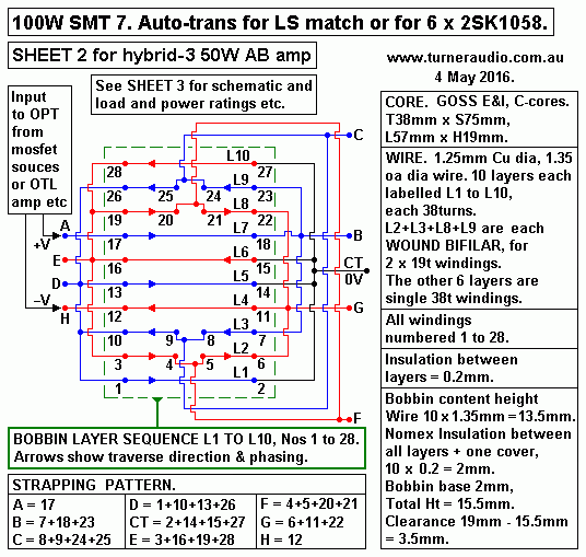
The OPT bobbin has 10 layers of 1.25mm Cu dia wire of which 4
layers
are bifilar wound. Insulation between layers = 0.2mm, and there
are 28
connections which should be connected as shown for best HF
performance
with all load values.
Fig 15. Hybrid - 3, SHEET 3, with SMT schematic and all
properties.
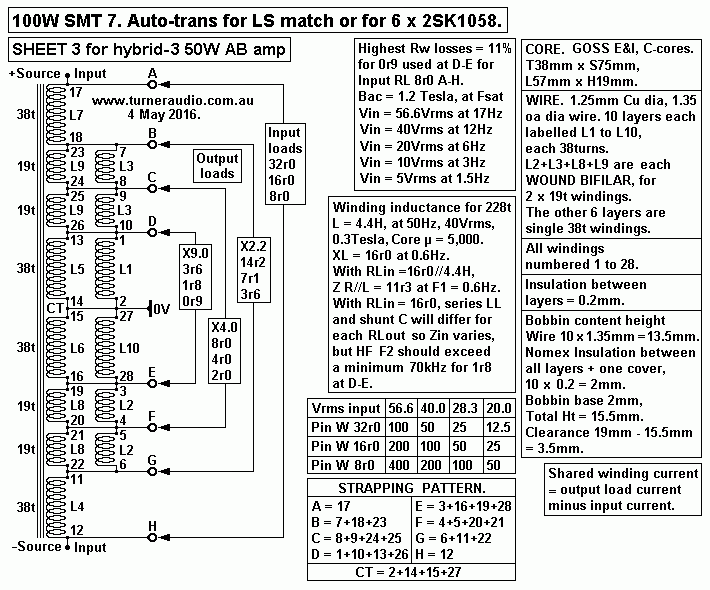
SMT 7 can work as a normal OPT with balanced Vac to each end of a
transformer input winding with a CT taken to B+ or to 0V.
For the amp in Fig 13, each input winding end is driven by
parallel mosfets in
source follower mode.
Although SMT 7 looks complex, it is simpler and slightly easier to
wind because
the wire size is larger and there are less turns. This auto OPT
acts like a speaker
matching auto tranny with taps to provide different load matches.
There are a
total of 10 layers of wire, numbered L1 to L10, with each layer =
38turns.
6 layers are in series to make the total input turns = 228t.
Another 4 layers are
in series to make 152t which are then paralleled to 152t of the
other 6 layers.
The interleaving and strapping and taps give low winding
resistance and good
HF performance for the desired range of output loads.
The positions of layers L1 to L10 in bobbin have no correlation
with sequence
of layers in schematic from bottom to top.
Confused? It does take some time before you cease making mistakes
while
trying to wind this OPT.
The terminals A to H on the transformer case should be clearly
labeled
with A to D all RED, and E to H all BLACK, so there is no
confusion about
The CT need not have any terminal on transformer case.
In addition to the 3 load Impedance Factors shown for X2.2, X4.0,
X9.0,
There is one more, X2.9 with either Then B - F or G - C which
gives 16r0 : 5r4.
---------------------------------------------------------------------------------------------------------
Fig 16. Hybrid - 3, SHEET 4, PSU for 50W AB amp.
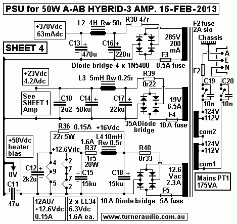
Fig 16 PSU needs no explanations, and many ppl may do something
different.
The PT should have VA > 175, and filtering Vdc should as good
as shown and
results should be good.
Fig 17. Hybrid - 4, Circlotron using tubes and mosfets.
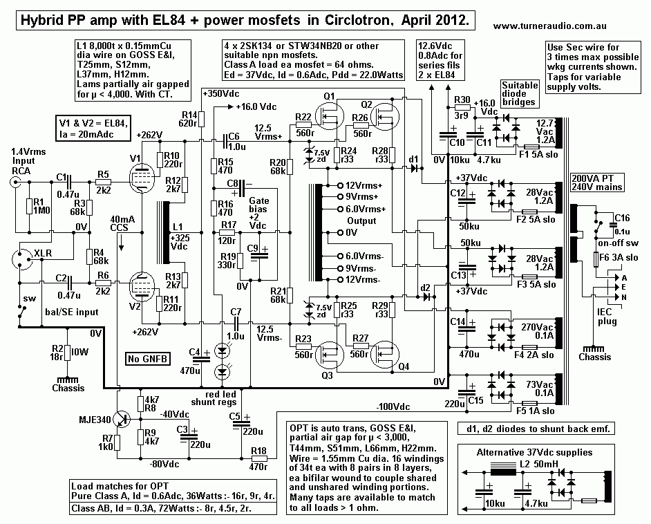
This Circlotron design was something I designed in April 2012
after
contemplating the designs of Susan Parker at her website where she
shows
the details for what have to be the simplest solid state
amplifiers ever
conceived by anyone.
See http://www.audiophonics.com/index.html
Susan has used CD player to volume control to drive an SE mosfet
in
source follower to drive a step up input transformer with balanced
output to
drive 2 N type power mosfets in class A and source follower which
drive
an OPT. Its about as simple as it could be with a minimum of
active devices,
and any HD generated by iron is minimized because the transformers
are
driven by very low output resistance of a source follower.
Many would argue transformers have no place with solid state
because
solid state was invented to get rid of the expensive heavy and
complicated
transformers, all so difficult to design and make. SS allows all
electronics far
lighter, smaller, and able to do 999 additional useful things like
making washing
machines electronically controlled, and emails that are cheaper
than telegrams
etc. But with music, solid state has never proved superior except
to provide
an easy way to make 250,000W for a rock concert for 250,000 kids
all
wanting to hear their favourite noise tunes at deafening levels.
If we wish to hear what one cello wants to sing, and how it wants
us to feel,
we can be forgiven a desire for a few Watts in Class A. And an
orchestra with
50 musicians will also sound very well with class A and tubes, and
perhaps
mosfets in class A.
Susan uses a simple OPT to couple mosfets working in balanced
source
follower mode and class A. Using balanced N channel mosfets in
class A gives
very low THD because the 2H cancels very well just like having 2
tubes in PP
class A with an OPT. I have considered the use of a Circlotron
because it
results in having a much lower drive Vac to mosfet gates,
and the amount
of useful local NFB is still very high and enough to keep Rout
quite low
enough for most speakers.
The other benefit of the Circlotron is that the loads of each 1/2
of the PP
circuit are in parallel, unlike the ordinary conventional PP where
the loads of
devices on each side of PP circuits are always in series, as in
Fig 13 amp.
And each 1/2 primary of a Circlotron OPT can be closely coupled
using bifilar
windings, and with mosfets, the Vac are all low and circuit
impedances low so
usually the transformer can be an auto-transformer with one
winding and taps
out for impedance matching. Capacitance does not cause resonances
near the
audio band and insulation may be thin and leakage inductance kept
low with much
interleaving AND multi-filar windings. Very wide bandwidth is
normal and easy
to obtain. In class AB, there are no windings where current is cut
off, as mosfets
on each side put power into all the OPT windings and input load.
Fig 17 has 4 mosfets, and there are TWO 37Vdc "floating B+
supplies" and
Id = 1.28Adc, so 0.64Adc in each mosfet. Idle Pdd = 37V x 0.64A =
23.7W. RL
for each mosfet in class A can be calculated as = 0.9 x Ed / Id =
0.9 x 36 / 0.64 =
50.65r, say 50r0. With class A the Id swing = +/- 0.64Apk, Po =
10.2W.
Vds for each mosfet = 22.6Vrms, and this is applied across the
whole OPT primary with its CT so you end up with +/- 11.3Vrms each
side of CT.
All 4 mosfets act in parallel to change current and voltage and
the load across
the whole transformer is 50r divided by the number of mosfets each
making class A
Po, so the transformer input load = 50 / 4 = 12r5, and with Vo =
22.6Vrms, you
get 40.9 W, class A.
If the transformer has taps at 0.67 and 0.5 of the whole winding
then output loads
may be 5r6 and 3r1 which usually make everyone happy with real
world speakers
between 3r0 and 16r0.
The pair of mosfets on each side of PP circuit provide oppositely
phased voltage
and current changes but they still act together to make the ONE
output voltage of
22.6Vrms across the OPT.
In Fig 17 schematic, I have shown the load on each mosfet as 64r0,
valid if a
16r0 is used across the maximum OPT winding turns. Now 64r0 is a
very high ohm load for any power mosfet, and the gain of mosfet in
class A and
amount of local source follower NFB is over 30dB, which means the
THD is very
low. Susan Parker has quantified the THD that may be expected
in her posted THD results, and THD is remarkably low.
In most mass produced amps using mosfet output devices, the load
on each
mosfet in nearly class B operation is usually 4r0 to 8r0. THD
produced may be
16 times higher than for the class A condition with 64r. Not only
that, with rather
unmatched N and P channel complementary pairs the THD of each is
different,
and because of such a low amount of class A there is little even H
cancellation
and the result can be said to be a "dingo's breakfast", aka sonic
horror, and then
to straighten out the mess the designers apply about 55dB of
global NFB.
Even I have done just this in my 300W amp with 6 mosfets.
But it does make a few first class A Watts which covers all I even
listen to, and
in fact the mosfet distortion including the reputably dreadful
crossover distortion
is not too bad with source follower connection and less than 1% at
250W without
global NFB.
The 4% THD one may see without GNFB is due to the CLASS A PP
balanced
driver stage where mainly 2H and 3H are made with very low higher
order H,
so the driver THD contributes most THD at 4% at 250Watts without
GNFB.
Harmonic mess without GNFB is no worse than using 6 x KT120 with
little initial
class A with low bias currents. 50dB of applied GNFB is typical
for a mosfet amp
and it is easy to have open loop BW extending to 5kHz. Using 50dB
FB means
reducing THD by factor = 1/ 3,000 so 4% becomes 0.0013%.
When one examines the error signal applied to mosfet gates it is
hard to see any
distortion which means there is very little error correction to be
done. With very
good power supplies with 2 rail caps of 100,000 uF each, noise is
extremely low,
and I know ppl who could not tell any difference in sound made
between class A
tubes and class B mosfets. The same man did the design though.
To conclude, where needed Po < 30W, class A is an easy path to
low THD/IMD
And class A plus high ohm loads with source follower OR
Circlotron, and enough
mosfets, their internal gain becomes high, and the amount of
follower NFB becomes
high enough to linearise the output signal so there is no need for
global NFB.
Fig 18. Picture of the 12.5W hybrid prototype amp with EL34
driver :-
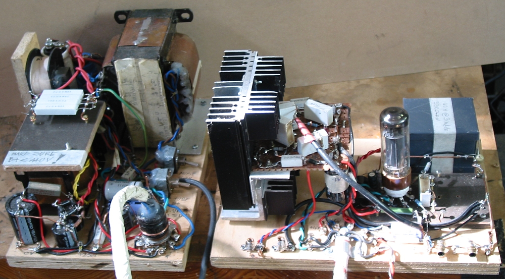
The above is a complete mess, but it worked well and proved my
ideas worked
well for all the Vo used as GNFB to a screen of EL34, which then
works like a
triode, but one which is a differential amp.
You may well ask how it is done. Its called the Complementary
Compound Pair
connection. at least 4 mosfets are used, 2 N and 2 P types, and
all have 1Adc
in all mosfets.
Fig 19. Hybrid - 5, Complementary Compound output stage.
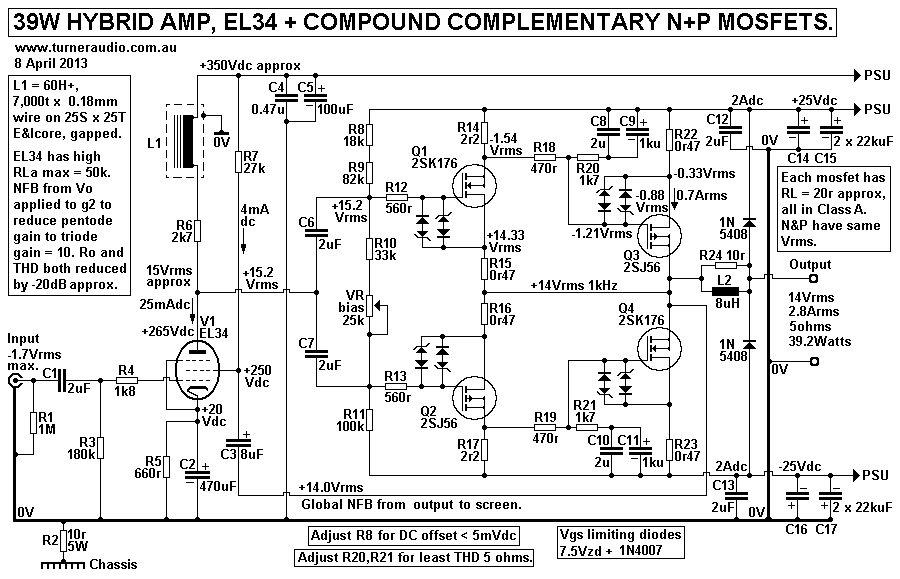
I have not built Fig 19 amp, but I see that use of both P-channel
and N-channel
mosfets working equally on each side of the push-pull circuit will
give better music
with lower distortion.
Q1 and Q2 are in complementary source follower mode but have small
loads
R14, R17 2r2 between drains and B+ and B- rails. About 50% of the
class A output
load current flows in R14+R17, and the Vac generated across each
2r2 is just
enough to generate about the other 50% of load current in Q3 + Q4,
arranged
in a complementary pair but in common source mode. This gives
symmetrical
wave shapes for the positive and negative 1.2 waves of any signal
because
both N and P devices are used in the same way. I believe the idea
may have
been invented by Crown, who made use of it in high Po professional
amps
with bjts working mainly in class B.
With Vo = 14Vrms, Po = 39W for 5r0, with all 4 mosfets sharing the
class A
load equally, and each mosfet works with RL of 20r. The class A
average Po
of each mosfet = 9.8W, with slightly less in Q1+Q2 followers and
slightly more
in Q3+Q4 in common source.The gate input capacitance to be driven
by the
EL34 ( or whatever other type of driver ) is kept low because only
two Q1+Q2
gates are to be driven, and follower connection reduces Cin <
200pF.
Fixed Vdc gate bias is applied to Q1+Q2 and their idle current
produces
Vdc across R14+R17, and the arrangement shows allows the idle DC
in all 4
mosfets to be controlled by VR-bias 25k, and regulated by the 4 x
0r47 source
R15,16,22,23.
R14+R17 set the Vdc biasing of Q3+Q4 gates and bias can be
slightly
adjusted further in Q3+Q4 by adjusting values of 2r2r slightly.
The R21 to R24 networks can be adjusted to get the right amount of
drive so
all 4 mosfets make the same power with at least the nominal load
value of
5r0. The above Vrms signal voltage figures are based on each
mosfet in class
A and gm = 0.8A/V. Voltage gain of each mosfet = gm x RL = 0.8 x
20 = 16x,
approximately.
If RL at output is lower, more current flows in Q1+Q2 source
resistors and
drain R15+16, and higher drive voltage is generated in drain
R14+17, and is
applied to Q3+Q4 gates voltage to increase current flows in Q3+Q4.
My thoughts are that after adjusting the 4 resistors for Idc bias,
DC offset,
and gate feed to Q3+4, the mosfets should remain stable for years
and not
need any further adjustments, so all adjustable R except bias
current level
would be done with pots. Pot ohm values are then measured and
fixed R of
correct value soldered in, and the whole circuit carefully
re-measured to give
equal current change in each mosfet and lowest distortion.
Some may use simulation programs. What would a simulation program
tell
you about the class A mosfet output stage as I have it? Other
types of N and
P channel mosfets may be suitable if they have a negative
temperature co-efficient
for the Idle conditions with Ed = 22Vdc and Idc = 1Adc.
More about heatsinks :-
As a rule of thumb, for each Watt to be dissipated you need 40
square
centimetres of surface area to prevent anything heating up to more
than 40C
in a room where room temperature is 20C. In other words, T rise
< 20C above
ambient room temperature.
40 sq.cm = 6.32cm x 6.32cm, or a square 2.5" x 2.5", 6.25 square
inches.
But if you want 40W of audio in class A then the heat sink must be
able to
transfer 100W of device idle heat to surroundings by combination
of radiation
and air convection.
For 100W heat transfer the area needed becomes 40sq.cm x 100 =
4,000 sq.cm.
Suppose you buy a heatsink that is 300mm long, 150mm high, with 30
vertical fins
each 40mm deep. Surface area total = 30 fins = 30 x 4cm x 15cm x
2sides =
3,600sq.cm, Base plate exposed surface area
= ( 30cm x 15cm ) + ( 30cm x 8cm total between fins ) = 690sq.cm.
Total = 4,290sq.cm. The amp case metalwork will also remove some
heat but it
also obstructs air flow, so never count on the case to help keep
things cool.
It is better to have washers between case and heatsink to allow
the heatsink to
work alone without the help of the case. The heatsink MUST be
mounted with fins
exposed to good natural airflow and the inside of case MUST be
well naturally
ventilated with perforated bottom cover, and holes near top to
allow air flow up
along inside area of heatsink using a gap of 10mm between edge of
any circuit
boards. This method allows Pdd = 100W with low T rise, ok for an
amp able
to make 45W in class A.
The 300x150x40 heatsink is otherwise suitable for a 300W class B
amp channel
as I used for an amp I made in 1996 seen here....
Fig 20. 2x300W stereo amp.
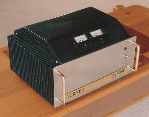
The idle Pdd in the above amp is 40W per channel, and it runs
slightly warm
after being turned on for an hour. This is how I like it.
Many will try to get heat sinks half the size to the above to
dissipate 100W
continuously - and they pay the price. Solid state circuits become
10% less reliable
for each 10C rise in temperature. So if T rises to 100C, expect
reliability = ZERO.
Happy thinking, soldering and listening.
Back to power amps directory
Back to Index page