MISCELLANEOUS
SCHEMATICS 2
DIY and other interested armchair experts might well wonder
what sort of schematics I have tried just for fun or to see if
they would hold promise because of their clever
novelty or special sonic characteristics.
WARNING!!
TUBE AMP CIRCUITRY REQUIRES EXTREME CARE WITH POTENTIALLY
LETHAL VOLTAGES.
YOU HAVE BEEN WARNED.
Please excuse the hand drawn circuit presentation of schematics
and file size.
M9. Basic Balanced Shunt FB; 2 x 6L6GC
M10. Balanced Shunt FB; 100W 4 x 6550 per channel
M11. Balanced screen FB, for 4 x 6550.
M12. Automatic servo bias control 1 or 2 x KT88 etc.
M13. Error correction in generic ultralinear PP amp
M14. Error correction fully balanced PP amp, 2 x KT88 etc.
M15. Line level preamp test, 2 triodes, THD graph.
M16. Simple line preamps with 2 and 3 triodes.
M17. Integrated line preamp with switched gain and CCS and 2
triodes.
---------------------------------------------------------------------------------------------------------
M9. Very Basic Balanced Shunt Feedback
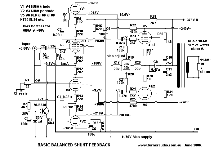
The Balanced Shunt Feedback amp was an idea dreamed up to exploit
the idea of applying balanced
loops of shunt NFB from the output stage tube anodes back to the
output of a balanced drive stage using a
long tail pair.
The feedback loops are the shortest loop available as they do not
include the secondary of the output
transformer, and avoids some of the instability and phase shift
effects of leakage inductance in the OPT.
To make things slightly clearer, here is an even more basic
simplified schematic circuit :-
M9a. Basic shunt FB diagram.
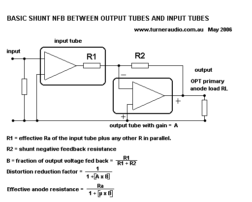
The problem with anyone wanting to design a shunt FB using NFB
between input and output and to calculate the
effect on distortion and output resistance is to work out R1 and
R2 carefully. Once that is done, all that is needed
to work out the distortion reduction factor is R1, R2, and output
tube gain for a given load value. We do not need
to know input tube voltage gain. And the effective anode
resistance after feedback has been added can also be
calculated. From these figures we can work out whether there
enough NFB or too much.
So let us analyse the above PP amp with 6L6.
The input LTP is arranged using the pentode sections of a pair of
6U8A triode-pentodes.
The triode sections are configured so they make a high impedance
load on the pentode at signal frequencies,
but at low frequencies they act to supply the required amount of
quiescent DC to the pentodes.
The input impedance to the triodes is high while the output
impedance from the triode cathodes is nearly as low
as a cathode follower.
There are feedback resistors of 470k between the 6L6 output tube
anodes and the pentode driver tube anodes.
When these are not connected, the gain of the driver stage is
extremely high because pentode gain is about
gm x RL, and the triodes above the pentodes have an equivalent
very high loading dynamic impedance.
In the case of the 6U8A triode section, µ = 40, so the effective
impedance looking up into the 22k cathode resistor
= [ ( µ + 1 ) x Rk ] + Ra = ( 41 x 21.2 k ) + 5 k = 874 k-ohms.
There is a 1M triode triode grid bias resistor but it is
bootstrapped off the 1k2 and 22k triode cathode R network
so the 1M is a load which is much higher than 1M so the triode
plus its cathode R act as a dynamic load of
approximately 800kOhms.
The feedback resistors between the output tube anodes and the
pentode anodes provide the driver pentodes with
their principle loads, equal in value to 470k divided by the
output tube stage ( gain + 1 ).
In this case output tube gain = 80Va / 9.5Vg = 8.42.
The voltage at the pentode anode = 9.8V since it always will be
slightly higher than the output from the triode cathode.
The amp schematic shows that +80V and - 9.8V appear at each end of
the 470k, so the official gain without follower
losses = 80Va / 9.8Va = 8.16, so the effective RL appearing
at the pentode anode is 470k / ( 8.16 + 1 ) = 51.3k.
Another way to look at it is to say there is a total of 89.8Vrms
across the 470k, so I = 0.191mA.
If the voltage at the pentode anode is 9.8Vrms, then its load = Va
/ IRL = 9.8V / 0.191mA = 51.3k.
However the loading of the triode stage has to be included part of
the load in parallel with the 470k effective load.
The triode loading = 800k, so the actual load seen by the pentode
= 51.3 // 800 = 48.4k.
The gain of the input pentode = µ x RL / ( RL + Ra ) .
It is difficult to know exactly what the value of µ actually is
because it varies because µ = gm x Ra and both the latter
change for a given value of Ia. But we can say that after perusing
the tube data sheets that gm = approx 2.8mA/V
and Ra = approx 400k. So µ = 1,120.
So the actual gain of the pentode = 1,120 x 48.4 / ( 48.4 + 400 )
= 121.
This is close to the above measurements in the schematic.
The tetrode output stage gain is approximately inversely
proportional to the RL. If the gain sags as a result of a lower
RL then the output anode voltage will reduce and the effective
load seen by the driver pentode stage will increase in
value, since 470 k will be divided by a lower ( gain+1) total. The
amp has RLa-a = 6k, and if RL = 3k, then the anode
signal voltage would fall from 80V to about 40V for a given grid
input signal so there would be 49.8V across 470k so
the I flow in the 470k = 0.106mA, and the load appearing at the
pentode = 9.8 / 0.106 = 92.5k. When this occurs,
the driver stage gain rises because its gain = gm x RL,
approximately, and more drive voltage is automatically applied to
the output stage grids via the low output resistance of the
triode's cathode above the pentode drivers.
The output impedance from the cathode of the triode is quite low,
and the following 6L6 grid bias resistors have little
effect on the pentode driver gain, due to the buffering effect of
the triode. This is important, since the circuit operation
depends on having a highest possible output resistance of the
driver tube which is the opposite of most conventional
ideas which say one should only use low mu triodes to drive output
stages. The arrangement of the circuit is negative
voltage shunt feedback. To make the most from the available NFB
the value of R1 must be kept as high as possible
and the value of R2 as low as possible without causing the driver
tubes to overload.
Beta, ß, the fraction of the output voltage fed back, is
calculated by working out the R1 and R2 resistance arms of the
basic shunt feed arrangement used in all shunt feedback circuits.
The R1 from input to the grids of the output stage
include the effective anode resistance of the driver pentode in
parallel with the triode current source impedance and
any other loads on the pentode except the NFB resistance R2 which
is 470k in this case.
The effective Ra' of the pentode = [ ( µ + 1 ) x Rk ] + Ra
= [ ( 1,121 +1 x 2.2k ) + 400k ] = 2.86Mohms.
In this case, R1 is equal to the triode dynamic impedance of 800k
// 3.86M = 625k.
and ß, the fraction fed back = 625 / ( 625 + 470 ) = 0.57.
Output stage gain = 80Va / 9.5Vg = 8.42
Distortion reduction factor , Drf = 1 / [ 1 + ( 8.42 x 0.57 ) ] =
0.172
Thus distortion of 3% without any NFB will be reduced to 0.517%
with shunt NFB.
An even greater reduction of output resistance/impedance, ie,
anode to anode resistance of the 6L6 output tubes is
available.
Without NFB Ra for one 6L6 = approx 35k, and µ = 200 approx.
Ra', after FB, = Ra / [ 1 + ( µ x ß ) ] = 35,000 / [ 1 + (
200 x 0.57 ) ] = 304r.
( This is less than 6L6 strapped as a triode = 1.6k. )
Now the OPT impedance ratio is 6k0 to 8r0, 750 to 1, so at the
output we would see the Rout
= ( Ra-a / ZR ) + total P and S winding resistance for the OPT
= ( 2 x 304 / 750 ) + Rw = 0.81ohms + approx 0.6 = approx 1r4.
The test amp had its total Rout = approx 1r3.
From the above calculations, any way we could increase the gain of
the output stage, and increase the value of ß by
having R1 as a higher value would improve the results
considerably.
In practice, getting ß up to about 0.5 is about all we could
manage, and using higher gain output pentodes,
such as EL34 or EL84, would make the circuit produce better
measurements.
Basically the output stage operates as an anode follower. A fuller
explanation of the principle is in the RDH4, pages
332 to 334, although they don't show the use of the mu-follower
circuit anywhere. The circuit also works well when
beam power output tubes are used in UL, but any output stage could
be drafted into this way of applied feedback.
The amount of NFB applied = 20 log ( 1 / Drf ) = about 15 dB in
this circuit.
The input pentodes and driver triodes can be separate tubes such
as 6AU6, 6BX6, 6EJ7 plus 12AT7 or other
suitable triodes. A separate heater supply biased at about 200 v+
for the follower part of the pentode & triode
series arrangement. To get the best from the circuit the OPT
should have low winding resistance, the output stage
should work in nearly all class A and the CT of the OPT should be
provided with a very well smoothed B+ voltage.
Where is any advantage to using balanced shunt NFB? I just cannot
see any for an output stage but it is an
interesting exercise to consider. Back in 1996 when I dreamed up
this schematic and tried it out on an old amp
chassis it was in response to Allen Wright's and Joe Rasmussen's
secret ideas of Forced Symmetry which used a
combination of balanced shunt NFB and balanced series voltage NFB
from the OPT anode connections back to
various points of the input/driver stage which I suspect consisted
of a long tail pair using two arms of j-fets and
triodes in cascode which make the equivalent of a pentode. I
recall discussing the whole idea of Forced Symmetry
with Joe in the editions of the news letter of the Audiophile
Society of NSW, A.S.O.N and I wasn't in agreement
with Joe at all. The Allen and Joe empire moved on to other
schemes to make their PP amps palatable to those
who thought single ended amps were the best. But please try things
for yourself before deciding what is best.
-----------------------------------------------------------------------------------------------------------
M10. Balanced shunt FB for 100W amp.
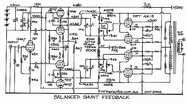
I have not built this amp, and I doubt I ever will because it is
too complex. I publish it here to
show where the idea for balanced shunt FB could be applied.
M11. Balanced screen FB.
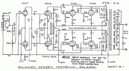
This schematic was used for awhile for an 8585 prototype but
abandoned for the circuit now
shown at 8585-amp-october-2006.html
But the balanced screen FB schematic worked fabulously well
technically but just didn't sound as later pages
for the 8585.
Maybe someone else could get it to sound better. The principle of
operation is simple enough.
The OPT has cathode FB windings where 12.5% of the primary
windings are devoted to the cathode circuit of
the output tubes. So there is about 8dB of local NFB applied in
the output stage. The driver input stage is a pair
of EL84 and are working in an LTP and in pentode mode and their dc
supply is via a choke with CT to allow a
high anode current without loading down the EL84 with a low value
anode resistance load.
The EL84 screens are not each bypassed to the cathodes of the EL84
but bypassed to the cathode feedback
windings of the OPT so that the voltage applied to the EL84
screens is about half the anode voltage output and
in effect there is approximately 12dB of series voltage NFB
applied back to the EL84 but to the screens instead
of FB to the cathodes via a low impedance resistance divider
network.
Hence the total applied FB is about 20dB and thd and Rout is nice
and low. But I later rigged the same amp with
the schematic shown on the 2006 8585 page and I thought the detail
and fidelity was better. The customer who
owned the amp I fiddled with at the time agreed with me that my
more conservative modification with global NFB
from OPT secondary to an SET input triode gave far better imaging
which he said was 3 dimensional. The use of
EL84 with choke loading in an LTP is a feature of all such
amplifiers I now make and in triode the EL84 is a very a
ccurate driver.
M12. auto biasing schematic.
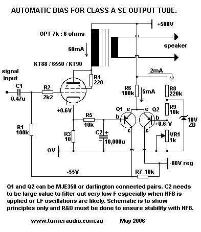
This schematic shows a basic idea for active servo bias control
for a single output tube. DC current in the tube
generates a voltage at R3. The signal Vac are filtered out by
R5/C2 LPF and the Vdc is applied to one the
base of Q1. The base of Q2 has a reference voltage of about
+0.6Vdc applied from the voltage divider
R8, R8, VR1. When set up, VR1 is adjusted to get the wanted bias
current in R3 10ohms.
Once the DC idle current is set, and changes to the cathode
current in R3 will alter the voltage at R3 and the
Q1base voltage. If Ik rises, then the voltage at Q1collector
will be driven more negative thus opposing any
rise in cathode voltage.There is enough differential dc voltage
gain in the Q1 / Q2 LTP to keep the idle current
in the tube constant once it is set.
This type of circuit can be developed to be used in a PP output
stage by having a slightly more elaborate LTP
arrangement which i found worked extremely well to control the
balance of dc current. Unfortunately when
even a small amount of global NFB is applied the circuit became
unstable at low frequencies and I decided the
complexity wasn't worth the benefits so this is another fine idea
I have never actually used. Perhaps someone
else might get it working better but I would prefer the simple RC
cathode biasing circuit which regulates the
bias current very adequately in class A amps. Sure there is some
wasted power dissipation in the cathode R
but the simplicity is worth the wasted heat.
This type of bias control is useless if used for class AB amps if
it is used to try to set the actual bias levels
because the cathode current changes and you don't want the grid
bias to change in class AB / B amps.
But where the LTP is set up to just balance the bias which would
otherwise stay fixed at the adjusted
value then the LTP does try to balance the DC cathode currents.
Trouble is, when NFB is applied such
circuits become de-facto phase shift oscillators.
---------------------------------------------------------------------------------------------------------
M13. Error correction in standard class A Ultralinear 30 watt
amplifier.
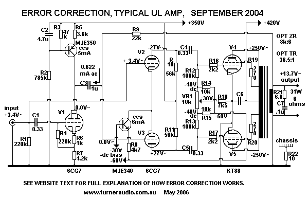
Considerable argument erupted at rec.audio.tubes when I published
this schematic at alt.binaries.schematics.electronic.
They all said it was just global NFB being applied in the same old
way, but they were all wrong.
The class A amplifier consists of a standard UL amp with KT88
(etc) and driven by an LTP. All the ac signal
voltages generated are shown with 13.7Vrms into 6 ohms at the
output giving 31W.
The differential input to V2 & V3 is +3.4Vrms, so the overall
voltage gain = 13.7 / 3.4 = 4.029.
The ac voltage shown have their phase polarity shown as + or - for
the instantaneous wave form condition.
The +input voltage is applied directly to the non inverting input
port at the grid of V2.
It is also applied to the input grid of V1.
One would think that since there is a CCS dc supply to V1 anode, a
healthy -voltage would be generated at
the anode. But V1 is set up so there can be as little as possible
output signal from its anode.
There is a 22k resistor, R9 cap coupled to the output of the OPT
secondary where the speaker connects.
The Vac at the output is +13.7Vac, so +0.622mAac flows from the
output to the anode of V1.
The V has the characteristics of µ = 20, Ra = 5k for the 2
parallel sections, and gm = 4mA/V
So since the anode output voltage is 0.0Vac, there must be a
voltage required at Vg-k to generate a current of
-0.622Aac to oppose the current in R9 so no anode voltage signal
appears.
This Vg-k required = I / gm = 0.622 / 4.0 = 0.155Vac.
So where we have +3.4V~ applied to the grid there must be 3.4V -
0.155V = +3.244Vac.
at the cathode, and since the ac Ia = 0.622mA, then Rk must be V /
I = 3.244 / 0.622 = 5.21k.
To bias the V1 properly for about 5mA of idle current and have a
dc anode voltage of about +120Vdc,
Rk must be divided into 2 resistors to derive a biasing voltage of
about -Vdc for the grid hence the Rk shown
above is divided into R6 = 1k and R7 = 4.2k. Thus far we have
calculated the values for the Rk to get zero
signal voltage output from V1 anode. In practice the R7 value
would be adjusted for minimum signal voltage
appearing at V1 anode when the load at the output is about the
middle value of load to be connected, and I
have chosen 6 ohms because it is about 1/2 way between 4r0 and
8r0.
So while there is 0.0Vac appearing at the V1 anode there is also
no signal voltage appearing at V4 grid.
Therefore the 3.4Vac input signal causes the full output to
appear.
The V1 anode output resistance = [ ( µ + 1 ) x Rk ] + Ra = [ ( 20
+ 1 ) x 5.2k ] + 5k = 114.2k.
This resistance acts with the 22k R9 to form two arms of a shunt
NFB network, and ß = 114k / ( 22k + 114k )
= 0.84.
If a distortion voltage +Vd appears at the output, then it is
divided by V1 Rout and R9 to give +0.84Vd at the
anode of V1 and hence is applied to the inverting port of the amp
which is the grid of V3. It is amplified by the
gain of the amp so distortion correction voltage at the output is
0.84 x 4.029 = -3.38Vd. This subtracts from the
distortion voltage of +4.438Vd which is would be present with no
error correction connected or if one simply
grounded V3 grid.
The distortion is thus reduced by a factor of Vd / 4.438Vd = 0.228
which is an applied error correction of 12.8 dB.
In math terms, the distortion reduction factor = 1 / [ ( 1 + ( A x
ß ) ] where A is the open loop gain without error
correction or NFB connected.
So in this case Drf = 1 / [1 + ( 4.029 x 0.84 ) ] = 0.228 which is
the same as the ready reckoning we worked
through above.
The effect of the error correction network on the output
resistance of the amp is the same as with a loop of NFB.
In this case the Rout without NFB would be 8r0, and the
transformed µ' of the output tubes at the output is
approx 0.7, so Rout' after error correction is applied = Rout / [1
+ ( A x µ' x ß ) ] where A is the gain of the driver stage.
In this case Rout' = 8 / [ 1 + ( 16 x 0.7 x 0.84 ) ] = 0r77. I
have neglected winding resistance of the OPT and in
practice Rout would be about 1r0.
So the error correction works to correct distortion and lower
output resistance in exactly the same way as NFB when
considering the math of how it all happens. But there is no
feedback signal voltage applied to the amp formed by
V2, V3, V4 and V5. By no feedback signal I mean a proportion of
the wanted undistorted output signal.
All normal FB amplifiers have a portion of their output signal ß x
Vout fed back and included in this signal is a portion
of the distortion at the output = Vdn x ß.
In a NFB amp the total applied input signal must be ( Vout / open
loop gain ) plus Vout x ß. If the above amplifier
were to be set up as a normal NFB amp and not use V1 at all then
to get the same distortion reduction factor we
would have to apply 11.5V~ of feedback signal to V3 grid and
14.9V~ to 2 grid.
Of course in practice this would not be done and V1 would be
utilized as a traditional gain tube ahead of V2&V3
and so a smaller feedback voltage and smaller open loop voltage is
used since the open loop gain would be much
higher for the amp. The error correction method involves less gain
tubes between input and output and employs the
error correction amp as an additional active amp to provide an
error correction voltage to be applied without any
wanted signal voltage to the main amp. It cannot be any worse than
having the extra gain tube in a conventional tube
line up.
T
he above amp is a bit insensitive with 3.4Vrms needed for full
power. But V2&V3 could be 12AT7, or a couple of
6BX6 or 6EJ7 strapped as triodes for some remarkable performance.
V1 could be a variety of triodes such as 6DJ8,
12AT7 etc. V1 does not have to ever produce much output signal
voltage and the values of Rk ensure whatever voltage
is produced is at low thd because of the local current NFB acting
with the Rk involved.
Time constants and stability issues may need additional phase
shift and gain tailoring networks to be applied as in a
conventional amp with global NFB Perhaps it sounds better with a
test signal by Beethoven, but to really find out,
build the circuit!
-----------------------------------------------------------------------------------------------
M14. Error Correction in fully balanced PP amp.
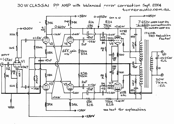
This schematic has a singe ended input converted to two oppositely
phased signals at the anode and
cathode outputs of V1. Signal voltages are shown as +V or -V to
indicate the phases, and instead of
having a balanced arangement of the single V1 in the 30W UL amp
above there is an arrangement
with the cross coupled four triodes to two balanced shunt feedback
networks shown as R1A & R2A, and
R2B & R2B to give very little signal output voltage at the
resistor junctions.
At the junctions there is only the correction voltage, ie, ß x
Vout where Vout is the anode signal at each side
of the output PP circuit. The schematic is a challenge for anyone
to build, as well as to understand. Rather than
say exactly how this works and put everyone to sleep, I leave it
to the few wide awake mortals with enquiring
minds to work it all out like I did.
There are many circuits for amplifiers which could be employed but
nearly all those like this last one are more
difficult to understand and are more complex and have a few more
triodes, R and C components than simpler
circuit topologies which have already been proven to work
flawlessly. So thus it would be difficult to justify
the extra complexity and the cost.
Some makers such as McIntosh and ARC do have more complexity in
their circuits than I would care to use.
These makers with very long established reputations are under no
threat from minor designers like myself who
would challenge the validity of complexity where I see no need for
it; I achieve splendid subjective fidelity and
quite good enough thd/imd measurements.
-------------------------------------------------------------------------------------------------------------
M15. Line level preamp test.
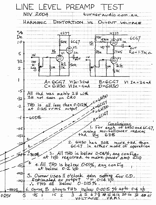
Please excuse the copy of the handwritten work book page I did
back in about 2004 when I measured
the THD for a line stage. The conclusions were:-
All triode types and configurations were acceptable.
6CG7 had less THD than the present fashionable flavor tube, the
6H30.
And BTW, my client thought the 6CG7 sounded better. I like 6CG7.
M15. More simple line preamps, 2 triodes.
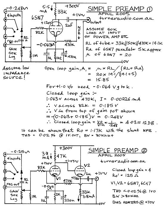
Here are a couple of simple line stages. Both 1 and 2 are
inverting amplifiers,
ie, the phase of the output is 180degrees to the input. Thousands
of
preamps have been made with the above recipes.
M16. More simple preamps, 2 and 3 triodes.
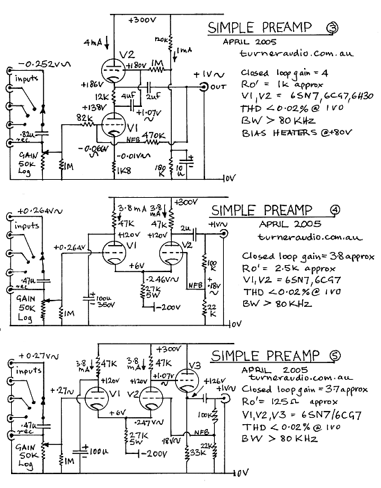
3 more line stages for examination. No3 is inverting, but types 4
and 5 are non inverting.
M17. Simple line preamp with CCS load loads for 2 triodes.
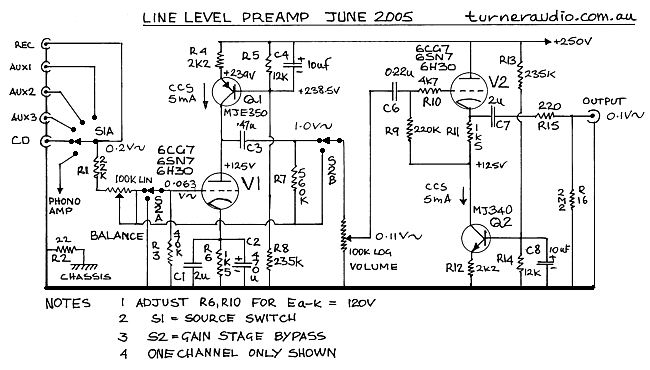
This inverting SET preamp has constant current sources for the dc
supply to both gain triode and cathode follower.
There is also shunt NFB around the input gain stage to reduce its
gain from being too high. The gain stage can be
switched out of the circuit when no gain is needed. 12AU7, 6DJ8,
6SN7 are all other suitable twin triodes.
Back to
Miscellaneous
Schematics 1
To
Index Page.