BASIC
TUBE 4.
Content..
About NFB within triodes, and much about power beam tetrodes and
pentodes.
Fig 1. Schematic Sheet A preamp to drive power tubes under test.
Graph 1. THD vs Vo for preamp, up to 120Vrms.
Fig 2. Schematic Sheet B for output tube testing, variable anode
loads and cathode biasing.
Table 1. Test results for 6550, fixed Eg2, beam tetrode mode to
determine Ra, µ g1, g1 gm.
Fig 3. 6550EH Ra curves, beam tetrode mode, 5k6 loadline.
Fig 4. 6550EH Ra curves, beam tetrode mode, 3k7 loadline.
Table 2. Test results for 6550 screen grid drive, fixed Eg1, to
determine Ra, µ g2, g2 gm.
Test results THD vs Va for :-
Fig 5. 6550 EH Tetrode, Ea = 335V to 347V. Eg2 = 321V or 231V. g1
and g2 drive.
Fig 6. 6550 EH Tetrode, Ea = 378V to 392V. Eg2 = 363V or 267V. g1
and g2 drive.
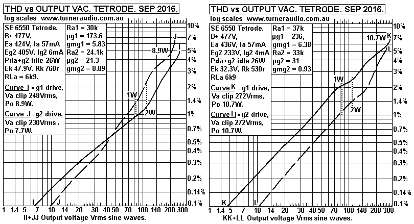
Fig 7. 6550 EH Tetrode, Ea = 424V to 436V. Eg2 = 405V or 233V. g1
and g2 drive.
Fig 8. 6550 EH Tetrode, Ea = 470V to 485V. Eg2 = 450V or 329V. g1
and g2 drive.
Fig 9. 6550 EH triode, Ea = 377V of 420V. g1 drive.
Fig 10. 6550 EH triode, Ea = 461V. g1 drive.
Table 3. Test results for 6550 EH triode to determine triode Ra,
µg1, gm.
Conclusions about beam tetrode and triode modes.
Fig 11. Schematic CCS instead of choke for test.
Some algebra.
-----------------------------------------------------------------------------------
Triodes have NFB inside them already....
Real triodes such as 6SN7 or 300B or triode connected beam
tetrodes and pentodes have
internal electrostatic negative feedback voltage acting between
the anode and the electron
stream and this is fully explained in Basic Tube 1 and 2.
For all beam tetrodes and pentodes with screen connected to anode,
the screen provides
much more transconductance than the anode to determine the
resulting low Triode Ra.
The screen grid is a second control grid using a helical wire coil
mounted on 2 support rods
and placed concentrically between the main control grid and anode.
Screen grids were designed to allow a fairly unimpeded anode
current flow of electrons
from cathode to anode, and yet the screen blocks most of the the
electrostatic field between
anode and any other grid between screen and cathode. A screen grid
needs to work at a
high enough +Vdc maintain a positive voltage field to attract and
maintain velocity of
electrons on their way to whatever is positive. Even if Eg2 =
+300Vdc, and anode is at say
+100V most electrons with increased velocity due to Eg2 field flow
past the fine screen wires
to the anode at the lower +V level.
During idle operation for beam tetrodes or pentodes, the screen
absorbs between 5%
and 30% of electron flow. But for power beam tetrodes or pentodes
the screen Idc is usually
about 10% of the anode Idc. During Vac operation of anode, a
screen with fixed Eg2 will
draw linear Iac from electron stream so the Idc flow from Eg2 rail
remains constant.
But at high Vac or Iac, the Iac flow to Eg2 rail becomes distorted
and at clipping the Ig2 dc
may be 3 times the idle Idc, and may cause the screen to overheat
if excessive Ig2 flows.
The tube data sometimes shows the increase of Idc input to g2
where Ea is low.
The anode Va can change over a wide range but with little Ia
change. The beam tetrode
and pentode Ra curves are nearly horizontal lines which indicate
Ea
can vary while Ia remains fairly constant. The Ra curves are
flattest for low values of Ia,
so Ra is a non linear property.
If you had a 6550 with Ea = +400V, Iadc = 60mAdc, you might think
Ra = 400V / 0.06A
= 6k6, and you would expect that if you changed Ea by +/- 100V, Ia
would change +/- 15mA.
But you could find Ia change +/- 3.3mA, so the resistance Ra
looking into anode
= 100V / 3.3mA = 30k. So we say that the anode has gm = 1 / Ra = 1
/ 33k = 0.033mA/V,
which is insignificant compared to the gm of screen grid2 with gm
about 0.8mA/V or control
grid1 with gm about 6mA/V.
But where a screen g2 has applied Vac in addition to its +Vdc
supply, we will find it has
substantial and useful ability to act similarly to g1 control
grid. For 6550, with Iadc = 55mA,
expect g2 gm = 0.8mA/V. If g2 is connected to anode for triode,
the combined effect of
anode gm and g2 gm = 0.033 + 0.8 = 0.833mA/V. We would then find
that if we altered
Ea by +/- 100V the Ia change = +/- 83mA, because Ra of triode has
become 1,200r,
ie, 1 / ( gm anode + gm g2 ).
WARNING. FOLLOWING TESTS ON TUBES INVOLVE HIGH VOLTAGES.
DO NOT ATTEMPT TESTING UNLESS YOU ARE FULLY EXPERIENCED.
To determine the properties of power tubes and to model their
behavior to better predict
the outcome in real power amps, a test circuit was built with Fig
1 SHEET A preamp and
Fig 2 SHEET B output tube test bed. The three parameters of Ra, µ,
and gm and the
requirements for biasing can all measured and calculated with the
test circuit.
There is a large choke with taps to feed Idc to the power tube
anode to allow measurement
of Ra with UL taps or cathode feedback effects.
Fig 1. Sheet A preamp.
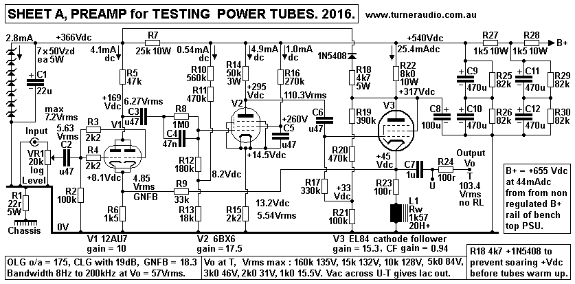
Fig 1 schematic is for a preamp to produce up to 135Vrms output
with B+ = +660Vdc.
The B+ could be lower where less output Vac is not needed. I
measured bandwidth of
8Hz to 200kHz at 57Vrms. Noise with VR1 turned low < 1mV for
Vac < 2kHz.
I found the amp adequate for all Va from tubes from 10Va to 300Va.
V1 12AU7 is a normal SET stage in differential mode with grid and
cathode inputs, to
allow about 19dB GNFB.
V2 6BX6 / EF80 is a sharp cut off RF pentode which has open loop
gain of 140, but is
reduced to 18.3 with un-bypassed R10 2k2. It has g1 bias from a
divider R10, R11, R13,
and R15 2k2 gives good local current FB and Idc stability.
V3 EL84 is cathode follower with Ia 25mAdc, and choke feed from
L1, about 20H at 1kHz,
with XL > 400k. R23 100r allows cathode Idc to be measured, R24
100r allows output Iac
to be measured at points U-T. The output resistance at T is about
130r.
7.24Vrms input is needed for 133Vrms output with a high Z load.
Load of V3 when not driving low resistance loads such as screen
drive is mainly R8 33k
for GNFB loop. Loading by most g1 input circuits of negative Vdc
biased output tubes
> 150k, so there is always enough Vout to drive all
output tubes to full Po.
The 3 tube pre-amp works from the non regulated B+ from my bench
top PSU supply,
about +660Vdc for the variable regulated B+ +380Vdc for the tube
under test.
When choosing regulated Vdc lower than +380Vdc, the bench top
PSU switches to choke
input type and its non regulated B+ drops to about +480Vdc. The
driver amp will still work OK,
but not make such a high Vo, OK because high Vac is needed with
output tubes set up to
work from +330Vdc or lower.
Notice the RCRC input filter or preamp B+ supply. This was
needed because the LF
noise in unregulated B+ from bench top PSU with LC filters is
quite high. I measured
transient noise Vpk-pk = 90mV, and this causes a high noise
level for low Vo from preamp.
The LF noise is generated by mains level changes and causes
change to anode Vdc
operating conditions of preamp tubes which then display a much
modulated level of THD.
The noise was too high without the good B+ filtering, with with
RCRC filters added the
noise floor < 1mV for F < 2kHz, quite good for any preamp
able to make 135Vrms.
Graph 1. THD for preamp.
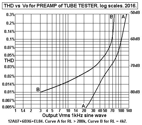
Curve A shows THD is a maximum 0.03% at 100Vac output where the
load > 100k,
typical for grid 1 tube input with a negative bias and a high
bias resistance.
The THD also depends on the ability to swing the voltage without
constraint of cut-off or
grid current in the V2 6BX6 or EL84 output tubes, and B+ for
above was +550Vdc, but
could be up to +650Vdc with . The The THD of preamp will be far
lower than any THD
in an output tube, and is mainly 2H, 3H.
Curve B shows the dramatic effect of driving a fairly low load
of the screen input
resistance which can vary between maybe 20k at low levels to 4k5
at higher levels.
The limit of Vac from EL86 cathode follower with low RLa 5k0 is
about 50Vrms when
peak Ik output equals the 15mAdc in EL86. If you wanted to
deliver 100Vrms into 5k0,
the idle current needs to be say 35mA, and choke needs to be
much bigger.
It would them be better to use an EL34 with Ea = 350V and
50mAdc.
Fig 2 below shows a schematic to test a range of power tubes
from small mini 7pin 6AR5,
mini 9pin EL84, octal 6V6, 6L6GC, EL34, KT66, 6550, KT88 to
KT150. Triodes such as 45,
2A3, 300B could also be tested although these have no screen
grid, and a DC heater supply
will need to be created.
For measuring triode properties of beam tetrodes and pentodes,
connect Screen g2 to anode,
and use the same method steps.
Fig 2. Sheet B for testing output tubes.
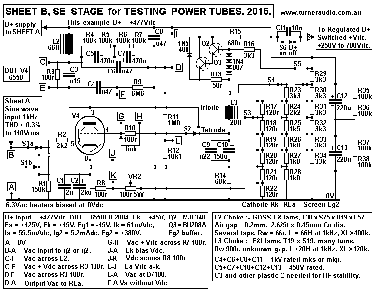
Fig 2 shows the anode load for tube under test consists of 4
parallel loads :-
(1) Choke L2 reactance, about 400k, (2) Variable RLa anode loads
R23 to R28,
(3) R6+R7 360k shown arranged to avoid Idc flow in RLa,
(4) Voltage Divider R11+R12 for 1M0 + 10k1 to allow 1/100
reduction of Va so
CR0, DVM, THD detectors have no effect on Va.
Also included in the load is series R3 100r, which is used to
measure Iadc and Iac
flow to anode. So we do not need to know the exact values of R
or of XL2 or anything else.
There is no need to try to calculate the load values before
measurements.
The approximate RLa value need only be known, and the range of
loads be between
about 1k0 and 10k0.
I found it most reliable to simply measure Va with DVM, then
measure Vac across R3
to measure anode Iac current. For calculations of Ra, the anode
current change and
voltage change for different loads must be known, and it is easy
to have 6 switched
RLa loads and write out 6 pairs of Iac and Vac results. When RLa
is calculated for
each position, it will not change much and where you want to
know RLa, you will have it.
L2 choke has two windings. One has 2,000t with a CT, the other
has 625t.
Both windings are used in series as shown to make just one
simple winding to
determine the raw data of Ra, µ, and gm. But later, I will show
effects of using UL
taps or for local cathode feedback (CFB) with 625t winding used
between cathode
and R&C biasing.
The resistors I used for anode load under S4 were from
accumulated old stocks taken
from junk I collected; they are not the exact values shown, and
are rated for a total of
100W at least. The same applies for variable cathode loads under
S3, and screen
voltage divider under S5. I have shown R values you may want to
use which might be
better than what I have used.
The unit allows measurement of Ra for any power tube and
configured in pure beam
tetrode or triode, or a suitable range of CFB or UL, by
means of measurement of two
Va and two Iac and calculating Ra = Va difference / Iac
difference.
S1a+b switches Vac from SHEET A preamp to grid g1 or to screen
grid g2.
Screen g2 characteristics are poorly understood by just about
everyone, but here we
can determine g2 resistance Rg2, µ, and gm.
Q2+Q3 form an emitter follower with low output resistance to
prevent Eg2 sag
during tests. The Idc input to a screen g2 remains fairly
constant at low Va but increases
rapidly over 2/3 of max Va to be up to 3 times idle dc at
clipping. L3 is a choke from
junk box with Rw 900r, and L well above 20H at low Idc. So the
total g2 supply has
output resistance < 1k0, low enough.
Plastic C with polyester mks or polypropylene mkp are used
across all electrolytic C
and a 0.15uF is across R3 100r. These C were all required to
prevent oscillation at
some very high RF which occurred when trialing triode
connections.
Earth wiring layout is very critical and must avoid any shared
0V rails of preamp
or output circuit. The schematics DO NOT show the exact layout,
and you must always
be able to perceive the presence of RF and eliminate it by means
of suitable shunt C
which do not lessen the wanted audio bandwidth. I found RF would
take some time
to begin, probably when 6550 had been left running for minutes
with a low load, and
grid 1 or screen had heated up a little. I then found THD much
increased and its level
would change while touching parts of circuit with a DVM which
has enough input C to
cause increase or decrease of RF.
For accurate tests, the series screen R10 must be bypassed with
a link which can be
removed temporarily to measure g2 Idc or Iac. Removing the link
while testing with Vac
the Va will drop slightly when R10 is not shunted, showing how
the slight Vac across R10
causes g2 gm effect on Ia. Where screen Vac drive is used to
determine g2 gm and g2 µ,
its Iac input resistance can be measured at points T-U at the
driver amp. In normal
power amps there are series screen R or grid R often used,
called "stopper resistance",
because they tend to stop parasitic RF oscillations. g1 R has
almost no difference to tube
tests but with added g2 R, calculations of gain for any real
power amp will always have
some error which becomes difficult to include in
calculations which then become too
complex to handle. We just need to know general principles, then
BUILD the circuit, and
how it sounds will depend upon our understanding of basic issues
rather than on our
ability to perform world beating mathematics.
The cathode is shunted to 0V via 2,000uF, which is 0.08r at
1kHz, and so with say
70mArms of anode current, Vk < 6mVrms and will give
negligible errors to our
measurements. Any real unbypassed Rk will increase the measured
Ra by about µ x Rk.
If the tetrode µ = 160, then Rk of 10r0 increases 32k Ra by 1k6,
causing error of 5%.
Hence I do not show any means of measuring Ikac, but I do have
means to measure Ikdc
at R8 100r J-K and to calculated the Rk value needed for any
Ikdc value chosen.
The screen g2 Idc can be calculated accurately enough by Ikdc -
Iadc.
The 0V rails in the circuit are 1.6mm dia solid copper wires.
The aluminium chassis
plate is NOT used for earthing, but is connected to 0V via 39r
5W. Metal cores and
holding yokes and tube socket brackets etc are connected to
chassis but are not directly
connected to 0V to help keep out noise.
While Testing Beam Tetrodes or Pentodes, a CRO ( oscilloscope )
MUST monitor
anode signal Vac to ensure THD is below 1% for measurements of
Ra, µ & gm.
To measure maximum single ended Po performance the anode loads
chosen are those
which allow maximum class A Po and anode efficiency for the Ea
and Iadc condition.
RLa load for beam tetrode or pentode = 0.9 x Eadc / Iadc.
RLa for triode connection = ( Eadc / Iadc ) - ( 2 x Ra ).
The display of THD on CRO allows the sudden large increase of
THD to be seen when
maximum Po has been reached at the onset of clipping. Generally,
I found this occurred
when THD reached between 4% and 5%. Very few tests showed there
was much useful
power when THD exceeded 6%. At such levels the output waveform
has departed from
a pure sine wave.
The example used here is a 6550 with range of Ea between +335
and +485V, and Eg2
between +267V and +450V, and with Iadc between 50mAdc and
90mAdc.
Idle Pda + Pdg2 is between 25W and 30W. In countless PP class AB
amps with 6550 or
KT88, Ea may be +424Vdc, and idle Pda will never be much more
than 1/2 the 42W Pda
maximum rating in data. The Ra, µ and gm all vary depending on
Ia, and if a 6550 idles
with Pda+g2 = 25W, it is in a comfortable position to give you
long tube life and plenty
of class A Po for 95% of most listening levels. The short time
Pda+g2 may reach up to
the 42W limit for a 6550 during transients or where a speaker
load is slightly too low.
There are extremists who insist on high idle Idc giving high
idle Pda+g2 near the data
limits and with output tubes at 100C above the "comfortable"
temperature.
Usually, there is no increase in fidelity for 90% of listeners.
The higher amount of heat
reduces tube life, brings larger electricity bills, and causes
more unforgivable greenhouse
warming.
The 6550 EH sample used was made in 2004, with about 500hrs of
use.
To determine Ra, µ and gm for any Ea and Idc idle condition, a
number of different
RLa values are chosen which are above and below the one load
value where maximum
Po may be produced. This load for max Po for SE pentode or beam
tetrode is calculated :-
RLa = 0.9 x Eadc / Iadc.
For example, a 6550 in beam tetrode mode with Ea = +424V and Ia
= 55mAdc,
RLa for max Po = 0.9 x 424V / 0.055A = 6,938r, or say 6k9.
Switch 4 allows selection of loads = 10k0, 6k7, 4k5, 3k0, 2k0,
1k0.
After the tube is set up for a desired idle Ea and Iadc and Eg2,
a low input grid signal
is used to generate a sufficient level of anode Va to allow easy
and accurate Va
measurement between anode and 0V, and also across the 100r
current sensing
between anode and Idc feed, and switched RL. The Va level needs
to be kept low so that
THD in Va is always less than about 1%, even with a low load,
where THD will be highest.
In Schematic Fig 2, the measurement of Va to 0V is done from
point F to 0V, and Vac
across R3 100r is done between point D and F.
THE ARRANGEMENT is SAFE because D and F are at 0Vdc, and
although high Vac
can be lethal the anode Vdc is best kept out of any Vac
measurements which could
damage meters.
To determine the Ra the Vac and Iac at anode is measured for at
least 2 different RLa
and with a constant grid input Vac. From the measurements of
gain for at least one RLa,
µ and gm can be calculated.
Ra = difference in Vac across 2 RL / difference in Iac for 2 RL
where the input
Vac is kept constant.
Table 1. 6550 Beam Tetrode, constant 1Vrms, g1 drive,
fixed Eg2.
Test
number
|
Ea
|
Iadc
|
Eg2
|
Ig2
|
Vg-k
Vrms
|
Va
Vrms
|
Ia
mArms |
RLa Va / Ia
calculated
|
Gain A
Va / Vg
|
1
|
+421V
|
55mA
|
+403V
|
5.9mA
|
1.000
|
41.58
|
4.36
|
9.537k |
41.58
|
2
|
"
|
"
|
"
|
"
|
"
|
32.83
|
4.66
|
7.045k
|
32.83
|
3
|
"
|
"
|
"
|
"
|
"
|
22.50
|
5.00
|
4.500k
|
22.50 |
5
|
"
|
"
|
"
|
"
|
"
|
15.86
|
5.37 |
3.969k
|
15.86
|
5
|
"
|
"
|
"
|
"
|
"
|
11.08 |
5.56
|
1.993k
|
11.08
|
6
|
"
|
"
|
"
|
"
|
"
|
6.029
|
5.54
|
1.088k
|
6.029 |
For all Vac measurements, my Fluke DMM
is accurate enough and gives at least 3
significant figures for all Vac between 0.5Vrms
to 500Vac. It reads fairly quickly, unlike the lower quality of my
Digitech.
Using results from test 1 and 2, Ra = Va difference / Iac
difference = 8.75V / 0.3mA = 29.17k.
Similarly, for
2 & 3, Ra = 30.38k,
3 & 4, Ra = 30.18k,
4 & 5, Ra = 31.87k,
5 & 6, Ra = 29.75k.
Obviously, there are "inconsistent & unexplainable" variations
in Ra which could be due
to meter reading errors and the variation of Ra. For calculations,
we are allowed to
average the results, so average Ra = 30.2694k, say 30.27k, or
30k3.
For these test results, Vg = 1.000Vrms, so gain = 41.58 with RLa =
9.537k.
µ g1 = A x ( Ra + RLa ) / RLa = 41.58 x ( 30.27 + 9.537 ) /
9.537 = 41.58 x 4.17389
= 173.55. Say 174.
Gm g1 = µ / Ra = 173.6 / 30.27k = 5.73mA/V.
If I increased Vin, I found I needed about about 6Vrms at grid 1
to get Va = about
250Vrms with maximum RLa load of about 10k. I try using Vg1 in =
3.000Vrms, but
found higher variation of Ra and a slightly lower average. The use
of 1.000Vrms input
is quite OK for most tubes providing your meters are accurate
enough.
From all this, we can see that Ra, µ and gm are not constant and
vary more widely
for higher Ea and Ia swings, so the non-linear character of basic
parameters impose
themselves. The values of Ra, µ and gm vary for every change of
operating condition
for Vac and Idc.
When we look at the data sheet Ra curves for a 6550 for values of
Eg1, the Ra lines
are anything but straight, and Ra is most horizontal for low
values of Ia, so Ra is
highest with low Ia, and the line slope increases with Ia so Ra
reduces. The vertical
distance between Ra curves varies for equal change of Eg1
which shows gm changes
with Ia. All this has to be accepted as being normal for a vacuum
tube or bjts or
mosfets and the only way to reduce the inevitable THD is by use of
NFB loops and
perhaps balanced Push-Pull connection which at least prevents even
numbered H
with same phase at each device from appearing at an OPT secondary.
Fig 3.
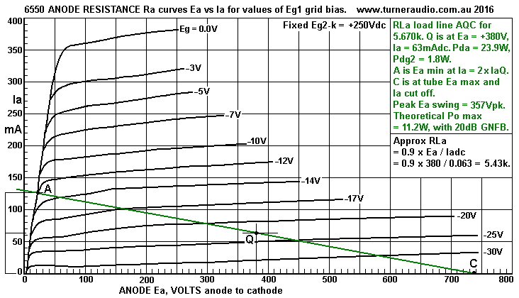
Here is an old set of 6550 Ra curves drawn originally by
Audiomatica, and one
glance tells you the curves LOOK HORRID because of inexplicable
irregularities in
shape of Ra curves. But the old curves are a guide, and a few
conclusions can be
made about tube Ra and grid g1 gm.
I show a load line for 5.67k A-Q-B. It is the graphically derived
RLa for maximum
theoretical class A Po.
This RLa = max Va pk-pk / 2 x Ia at Q = ( 737V - 23V ) / 0.126A =
5,666r.
The +/- Va swings are assumed to always be equal for the RLa for
maximum Po.
All other load values give less max Po where limited by max THD =
5%.
The Ra lines are not straight and Ra value varies along each point
along each
Ra curve for small changes of Ea swings. But to seek a usable Ra
value from
curves we draw a STRAIGHT LINE through Q and approximately
parallel to nearest
Ra curves.
I show this as Ra-Ra, and it is parallel to Ra curves for Eg1 =
-20V and -25V for a
voltage distance of 100Vpk each side of Q. The Ra-Ra line was
drawn manually
after holding ruler across laptop screen and putting a dot at each
end,
the R value = V change / I change.
From looking at the Ra curves, Ra = 30.55k and gm g1 = 6.2mA/V,
so µ = gm x Ra = 0.0662 x 30,550 = 189. It is impossible to
accurately
determine THD from any beam tetrode or pentode Ra curves with a
drawn loadline.
All you can do is assume that no matter what RL or operating point
is chosen, there
will be high THD even at 1Watt, with both even and odd H produced
in THD.
The gain = 189 x 5.67 / 36.22 = 29.6, and only 8.6Vrms is needed
at Vg1-k for full Po.
For Hi-Fi, we could reduced the gain by a UL tap and perhaps a CFB
winding to give
Vg1-0V = 50Vrms, and we would find THD was 4 times lower, with
little odd H,
less than triode, and and output stage output resistance also less
than triode.
Notice that I have applied the formula RLa = 0.9 x Eadc / Iadc =
5.43k.
This is slightly less than the graphical method of RLa prediction.
But not all tetrodes or pentodes have a diode line so steep as
shown, at left side as
160r up towards right from 0.0V and 0.0mA. the diode line for UL
connection of CFB
usually shows a higher R value so the calculated RLa for max Po
may more closely
follow the graphical RLa. The Po predicted = 11.2W, which is 46.8%
of idle Pda, a
theoretically good result. In practice, the distortion may reduce
Po max, and if an
SE OPT was used, maybe you will not get more than 10W at OPT
secondary.
Fig 4.
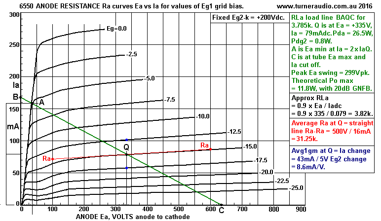
Fig 4 shows a SE 6550 with lower Ea at +335V and Ia = 79mAdc, and
Eg2 is at a
low 200Vdc.
Notice that the "knee of the Ra curve" for Eg1 = 0V is about
250mA, much lower
than in Fig 3 with Eg2 = 350V, and knee at 350mA.
The lower Ea and higher Ia and slightly higher Pda and lower Pdg2
means the
load can be lower at 3k9. The calculated RLa = 3k8, hardly any
different.
From Fig 3 and Fig 4, there is a load range between 5k7 and 3k8,
for Ea between
380V and 335V, so that it becomes possible to design an amp's B+
to suit the load
value proposed.
Most music listening uses Po less than 10% of the maximum at
clipping.
So if a tetrode makes 10W max, then most listening is done with
under 1W, and this
means Va = 0.316 x maximum, or say 70Vrms, well below max at say
220Vrms.
Therefore we can use nice simple formulas with ONE value for Ra, µ
or gm calculated
from measurements using Vin at g1 = 1.000Vrms for most beam
tetrodes and pentodes.
But for triodes, or UL, or CFB, or screen g2 drive, the input Vg-k
will need to be
increased to get similar Va-k figures listed in Table 1.
---------------------------------------------------------------------------------------------
Now for what seems quite odd, Screen Drive, with a fixed Eg1.
In effect, screen drive converts the beam tetrode or pentode to
triode operation where
the Ra remains nearly as high as form tetrode or pentode and the
gain is quite low
because the screen has quite feeble transconductance compared to
the control grid g1.
The values of Ra, µ, and gm may be derived in the same as for g1
drive above.
Table 2. SE Beam Tetrode, Screen g2 constant 5.00Vrms
drive, with fixed Vg1.
Test
number
|
Ea
|
Iadc
|
Eg2
|
Ig2dc
|
Vg2-k
Vrms
|
Va
Vrms
|
Ia
mArms |
RLa Va / Ia
calculated
|
Gain A
Va / Vg2
|
1
|
+424V
|
55mA
|
+387V
|
5.2mA
|
5.00
|
31.33
|
3.29
|
9.523 |
6.266
|
2
|
"
|
"
|
"
|
"
|
"
|
24.58
|
3.49
|
7.043k
|
4.916
|
3
|
"
|
"
|
"
|
"
|
"
|
16.79
|
3.73
|
4.501k
|
3.358
|
5
|
"
|
"
|
"
|
"
|
"
|
11.80
|
3.88
|
3.041k
|
2.36
|
5
|
"
|
"
|
"
|
"
|
"
|
8.22
|
3.98
|
2.065k
|
1.644
|
6
|
"
|
"
|
"
|
"
|
"
|
4.46
|
4.10
|
1.087k
|
0.892
|
I calculated 3 Ra values for results
with 1&2,m 3&4, 5&6 to get
33.75k, 33.27k, 31.33k, with average Ra = 32.78k.
µg2 = A x ( RL + Ra ) / RL. Using test 1, µg2 = 6.266 x ( 32.78 +
9.523 ) / 9.523
= 27.836.
gm g2 = ug2 / Ra = 27.836 / 32.78k = 0.849mA/V.
The tests were made series screen R10 shunted by link.
After these tests to determine Ra, µg2, gm g2, R10 had its shunt
link removed
to measure screen input resistance which varied from about 7k0 to
4k0.
These tests determine screen g2 gm, something we should know for
gain
calculations for UL or CFB.
For most calculations, the Ra calculated for beam tetrode may be
be use for
screen g2 drive. Only one amp designer ever produced a
manufactured batch of
hi-end amps with screen g2 drive. It was Tim De-Paravicini at EAR,
and the amp
was SE, using a rare tube which had a relatively high screen g2
gm.
To keep it linear, it used cathode follower drive to g2, and 20dB
GNFB.
With 1.000Vrms drive to g2 in 6550 with 100r R10, I measured Rin
g2 = 7.7k with
RLa 9.5k, and Rin g2 = 12.5k with RLa 3.1k. The g2 input
resistance is LOW, and
varies with RLa value and the level of operation, and input
current is needed to
produce a larger output current, and this mimics the operation of
a transistor !
Unfortunately, this means the output signal and loading modulates
the screen drive
signal so it is essential the driver is a cathode follower with
Rout < 500r if possible.
So an EL34 would be needed to drive a 6550 g2. 99.99% of
manufacturers would
avoid screen drive because a power tube must be used for each
screen to be driven
and the output circuit has low gain and high Rout so there must be
20dB GNFB.
There is not much headroom for any boosting of Vg2 by NFB to keep
Va constant
with a low value RLa. It is always far easier and more effective
to boost the grid Vg1
to maintain a low Rout. However, when g2 is driven by the anode of
the beam tetrode
or pentode, as in case of triode connection, or where g2 is driven
by a UL tap on an
anode winding there is a huge and useful reduction of effective
Ra. In CFB, if the g2
is held at 0V and a healthy amount of cathode FB is present,
the Vg2-k Vac is high
enough to give useful reductions of THD and Ra.
Here are some results of tests for THD vs Va for 6550 beam tetrode
with g1 and g2 drive.
Fig 5. Ea = 335V to 347V.
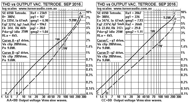
Average THD for g1 drive at 1W = 2.1%.
Fig 6. Ea = 378V to 392V.
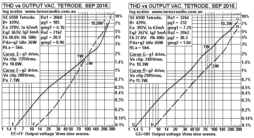
Average THD for g1 drive at 1W = 1.8%
Fig 7. Ea = 424V to 436V.
Average THD for g1 drive at 1W = 1.7%.
Fig 8. Ea = 470V to 485V.
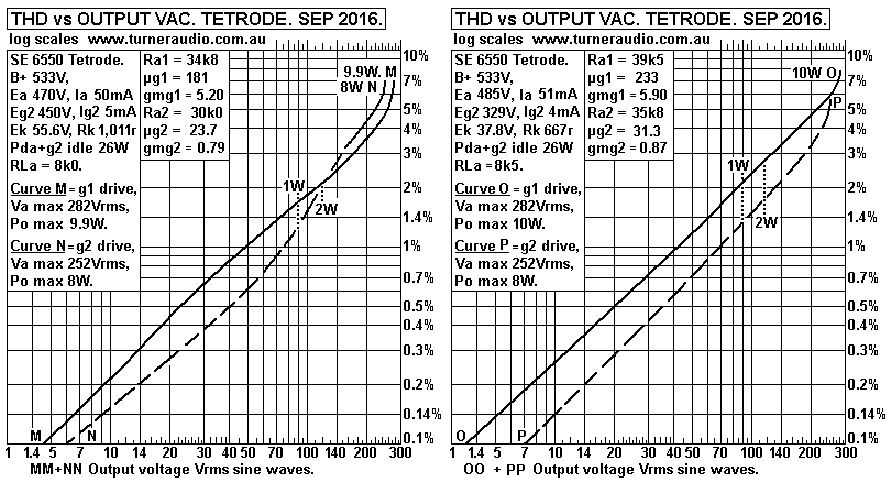
Average THD for g1 drive at 1W = 1.85%.
In all these tests you can see that THD at 1W is no less for where
Eg2 is considerably
lower than Ea. However, I observed THD was mainly 2H where Eg2 was
lower so the
conclusion is that beam tetrode THD can be very low for push-pull
class A operation
with less 3H and 5H if Eg2 is lower than Ea. But the Ra for
tetrodes or pentodes is
always many times the RLa value so adequate external loop NFB
connection is
essential for Hi-Fi with at least screen UL taps, preferably 50%
for 6550.
( 50% was used by Leak to good effect ).
The screen drive was tried for each of the 8 different Ea and Eg2
tests.
It appears the g2 drive "falls apart" where the Eg2 is close to
Ea.
Possibly, g2 drive could be more linear than indicated if Eg2 was
no more than
1/2 Ea for all tests. But the applications for g2 drive seem quite
pointless because
the better pathway to Hi-Fi involves an OPT with CFB windings of
at least 12.5%,
and possibly additional UL taps, and use of g1 drive. This
principle applies to both
PP and SE amps.
Fig 9. 6550 Triode, Ea 377V or 420V.
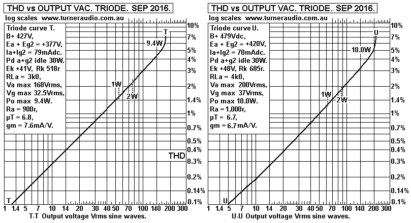
Fig 10. 6550 Triode, Ea 461V.
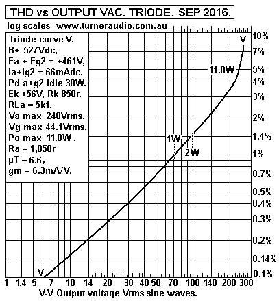
The THD for SE 6550 triode at 1W = 1.5% for 3k0, 1.2% for 4k0,
and 1% for 5k0, and overall triode THD is only -3dB less than pure
tetrode.
But the huge advantage of the triode connection is that the triode
Ra gives damping
factors of 3.3, 4.0, 4.85 for the 3 tests. Therefore the GNFB need
only be 12dB to get
THD to be always less than 0.31% at 1W, and the music should be
very good,
with DF further increased to over 12 in each case.
Push pull connection of 2 triodes with 12dB GNFB will give 0.02%
at 1W.
The success of the triode connection depends a lot on the
linearity of input and driver
stage because the 6550 triode maximum peak Vg-k = Eg1 bias, so for
the 3 tests the
Vg-k max = 29Vrms, 34Vrms, 40Vrms, a lot higher than for tetrode.
The THD for SE triode is mainly 2H, and its rate of production is
always much higher
than the 2H production by a triode driver tube such as a 6CG7,
which may only make
2% 2H at 40Vrms. However the phase of driver triode 2H will always
cause 2H reduction
in a triode output tube, so that 5% 2H at 90% full Po is reduced
to say 3%.
The 2H reduction at 1W is negligible. Input triode 2H has a phase
which adds to the
level of 2H in output triode, so thus it needs to be very linear.
Table 3. SE 6550 Beam Tetrode, Triode connected, Ea = +377Vdc.
Test
number
|
Ea
|
Iadc
|
Eg2
|
Ig2
|
Vg1-k
Vrms
|
Va
Vrms
|
Ia
mArms |
RLa Va / Ia
calculated
|
Gain A
Va / Vg1
|
1
|
+377V
|
72.8A
|
+377V
|
6.2mA
|
5.00
|
31.05
|
3.27
|
9.486k |
6.210
|
3
|
"
|
"
|
"
|
"
|
"
|
28.31
|
6.32
|
4.480k
|
5.662
|
5
|
"
|
"
|
"
|
"
|
"
|
23.63
|
11.51
|
2.052k
|
4.727
|
Using tests results 1 and 5, Ra = (
31.05V - 23.63V ) / ( 11.51mA - 3.27mA ) = 900r.
µg1 = A x ( RL + Ra ) / RL. Using test 1, µg1 = 6.21 x ( 9.486k +
0.90k ) / 9.486 = 6.8.
gm g1 = ug1 / Ra = 6.8 / 0.9k = 7.6mA/V.
Conclusions about performance of beam-tetrode and triode.
This series of THD graphs show that average THD for SE triodes is
only slightly
less than for beam tetrode operation. However triode connection
reduces the high
Ra of the beam tetrode by a factor of 0.1 to 0.03. This is
entirely due to the NFB action
within the beam tetrode due to the screen gm.
Although the Ra is hugely reduced to produce a good damping
factor, the screen gm
changes over a wide range Va and the feedback network is not
linear, so THD is not
reduced as much as NFB equations might calculate. At least the
screen NFB has a
bigger effect to reduce odd number H and the triode has
predominantly 2H.
Thus triodes will always work well in class A where a pair of 6550
can be used to
produce 20W in class A with 1% THD, mainly 3H, and at 1W expect
THD = 0.2%,
without global or any external loop FB. I have never heard a bad
sounding class A
triode amp.
Beam tetrode operation generates far more odd number H which
cannot be cancelled
by PP connection, so a class A tetrode amp with same idle Pda as
for triodes may
produce the same 20W with 4% THD. But it varies with load value,
and relative phase
of 2H changes with load value, and inescapable conclusion is that
beam tetrode or
pentodes cannot match the low PP THD of triodes. The tetrode or
pentode circuit MUST
have about 12dB global NFB or local CFB to match the triode
performance including
both low Ra and UL operation does allow low THD as low as triode
and with favorable
H content, but loop FB is still needed.
------------------------------------------------------------------------------------
Construction conundrums for test circuits.
The tube tester circuitry for Fig 1 and Fig 2 was originally built
before 2005 to estimate
how much SE Po and THD I could obtain from 3 x 6550 or EL34 in
parallel.
The large choke L2 = 5Kg, and has 2,625t around E&I gore with
T38 x S57.
The air gap was originally 0.5mm, and for Bdc = 0.6Tesla, with
240mAdc,
the core µe ( effective permeability ) = 158, giving a theoretical
L = 14.2H.
This meant the amp load RLa could be 1k8 where XL = Ra at 20Hz, OK
for where
there were 3 output tubes with each one loaded by 5k4, and able to
make 30W+, with
Iadc for the 3 tubes = 220mAdc+.
But I have reduced the air gap from 0.5mm to 0.2mm, ( with 2
sheets of paper
each 0.05mm, across the TWO joins in E&I lams.) This had the
effect of increasing
L to 66H at low Vac levels and with Ia = 60mAdc. I should be able
to use this beautiful
big brute of a choke to accept a flow of 100mAdc, where Bdc might
reach 0.6T, and
allow Bac = 0.6T for max Va = 300Vac.
There is now no need to test more than ONE tube, and Ia max could
be 100mA.
There is also no need to test tubes at low frequencies.
I am testing just ONE 6550, which has so far not needed Ia >
80mAdc. XL reactance
= 414k at low levels. This does reduce slightly to 330k where Va =
335Vrms at 1kHz.
Because we are NOT trying to examine voltage gain without any
load, ie, RLa = infinite
resistance, ie, a constant current source, the L for Idc feed need
only be 10 x highest
RLa which is to be used. In this case, RLa < 10k0, so XL can be
100k. The slight phase
shift and tiny amount of attenuation by parallel inductance will
not affect measurements.
The Ra of any tube tested could be 100k, and measurements to
obtain Ra are
determined by the range of loads not exceeding 10k0. The current
sensing R3 100r will
automatically include all Iac from RL, R dividers, shunt L. If Ra
was infinite, then the
change of load is exactly proportional to gm g1 x RLa, but we
never see this in practice
and always the load current changes for a constant Vg input hence
Ra can be calculated
and measured without interpolations of difficult old data graphs
of Ea vs Ia with Ra curves
which are notoriously vague and inaccurate for low levels of Ia in
a range between say
0.0mA and 500mA.
Understanding tube properties requires :-
(1) Cautious appreciation of the tube data Ra curves for "average
Ea vs Ia characteristics",
where every point of any line means a value of resistance, with
the curve showing how the
R varies. Ra curves for beam tetrodes at wanted low Iadc
conditions are often missing from
data sheets, or what is drawn was done by fairies.
(2) Serious test gear to measure Ra, µ, gm for all electrodes
which have these properties,
and how they affect gain and output resistance and distortion.
(3) Be prepared to discover that 2H distortion for triodes may be
less than curves indicate.
This probably means the test gear used to draw the lines on paper
before 1965 was
getting old, all the circuits used to drive a curve plotting
machine were tubed, and
controlled by NFB loops to make them more linear than anything
being measured
- if of course that machinery was serviced properly. The old
curves are wondrous
documents despite their slight inaccuracies. My father's
generation did very well with no
computers of pocket calculators, or digital voltmeters which
always give at least 3
significant figures.
With much effort, the DIYer or tube amp maker might just lessen
his ignorance.
I made the PSU
with Vdc
regulator some years ago and it has a range of
regulated B+ up to +581Vdc. There are 6.3Vac heater windings and
a variable -Vdc
for bias if needed. This PSU is a little too hard to build for
most DIYers; I took a
month, but I had enough experience to design and build something
using many
accumulated parts laying around.
DIYers could possibly make a normal B+ PSU capable of up to say
+600Vdc
working using a 300VA PT with 240Vac primary and 240Vac sec.
240Vrms from a HT winding can make +672Vdc unloaded with a
doubler rectifier
using 2 x 6A Si diodes to put up to +336Vdc into two 470uF caps
in series and each
rated for 350Vdc. A following LC filter will need a 5H choke at
150mA and Rw < 50r.
The following C can be any number of series 470uF caps but with
only 2 the 100Hz
Vripple with 100mAdc is less than 2mV. However, the mains level
is always varying
+/- 50mV because everyone connected is turning gear on and off,
and the +/- 50mV
mains change means Vdc at a doubler will change +/- 140mVpk.
The mains creates most noise during the day, but may be slightly
less at 3AM.
You may think its easy to rig up a non regulated B+ supply, but
I found the LF noise
of CLC filtered rails was a confounding nuisance, hence my
efforts to regulate the B+.
For example, where there is considerable B+ LF rail noise, the
measurement of THD
at low levels becomes inaccurate because the level of THD is
amplitude modulated by
the LF noise, and no filtering can be used to remove the H
content variations between
2kHz and 10kHz. The B+ rails MUST be regulated if you want a B+
rail which varies
less than -5Vdc for Iadc increase of 100mAdc at any B+ level.
One simple method for B+ adjustment uses a 400VA Variac to drive
the input of a
mains transformer with doubler after its secondary. As long as
Idc wanted is less than
150mAdc, you will not smoke the Variac but I suggest you MUST
HAVE a fuse on
Variac output to prevent it cooking if there is a shorted
output.
But for those with more time than money, it may be easier to
build a PSU with
300VA PT with HT = 500Vac max with say 12 taps at 35Vac steps
down to 80Vac,
and with a bridge rectifier you get +700Vdc max down to 112Vdc
in 50Vdc steps.
A very good quality 12 position rotary switch is needed with 3A
rating.
DO NOT use a cheap small signal wafer switch.
Instead of having a series regulator schematic as I do which
allows up to
300mAdc output, a shunt regulator can more simply be devised for
each chosen
B+ level so that 100mAdc can be allowed to flow in shunt
regulator without any load.
But if the regulated B+ = +600Vdc and there is no tested device
connected, then
the regulator devices plus series R will generate 60W, and the
typical bedroom
DIYer will never experience the luxury of a quite B+ rail with
output resistance < 20r,
and ability to instantly switch from a wide range of available
B+ levels.
Should anyone try to make a noise free B+ rail with CLC
filtering for up to 100mAdc,
consider CLC with 235uF + 100H + 2,350uF. There will be
unavoidable noise between
0Hz and 20Hz at 235uF, with 2 series 470uF. But the 100H plus
2,350uF has
resonant Fo = 0.33Hz. The XC = XL = 205r at 0.33Hz. If the choke
Rw = 205r, then
there is critical damping to prevent peaking of noise at 0.33Hz,
and at 3.3Hz there
is -40dB attenuation. The 2,350uF may be 20 x 470uF. For the
total of 22 x 470uF
at $20 each, its $440. The choke would cost at least the same,
and slow B+ changes
below 0.33Hz will not be prevented. For chokes, see my choke designs.
You could use an alternative to choke L2. it will be a Constant
Current Source,
CCS, which gives Idc which is determined by the Rk of the tube
under test, but the
ac impedance at 1kHz will have a finite R value > 500k.
3 x HV rated power mosfets could be tried :-
Fig 11. CCS for anode feed with B+ up to +800Vdc.
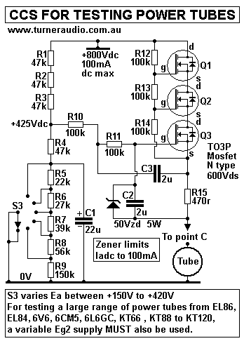
This little simple schematic should only take 4 Sundays to make,
allowing
for 20 mistakes and smoke events DIYer might make.
But my mistakes taught me so much.
This CCS does have some redeeming features. The 3 mosfets are a
source
follower with low Rout for Vdc at bottom R15. The Vdc out is
determined by the
selected Vdc at S3. The B+ Vdc variation is reduced by divider
action of S3,
but C1 22uF works with resultant 95k of parallel R to give a
pole at 0.08Hz,
so that B+ noise at 0.8Hz is reduced by 1/10. At 8Hz, B+ noised
is reduced by 1/100.
But at 1kHz, C2+C3 have XC = 80r, producing 0Vac between Q3 gate
and bottom R15,
thus preventing much change to Vac across R15, so the Iac output
is extremely low,
and less than 0.5mAac where Va of a tube is say 250Vrms,
assuming the finite Rout
at 1kHz = 500k.
Consider a 6550 with anode Vdc = +400Vdc at idle, with cathode
biasing Ek = +40Vdc.
The Ea = +360Vdc, and maximum peak Va in tetrode mode may be +/-
345V,
so the Va max = 400V + 345V = 745V. This is just accommodated by
the B+ input
= +800Vdc.
To allow a greater Va peak swing where anode Vdc is higher will
involve having B+
= twice the Vdc at anode, so if anode Vdc = 500Vdc, then B+ at
top of CCS needs to
be +1,000Vdc. Suddenly, what seems like a good simple idea
becomes a nightmare,
and damned dangerous.
The inexperienced DIYer may hate winding any choke. He may also
hate paying
for 4 small chokes of say 20H each for 100mAdc, so he might
connect them is series
to so what my big L2 can do. Making this CCS with Vdc rail at
800Vdc or more could
easily result in electrocution. It is very difficult to avoid
all shocks, and the non serious
DIYer will soon learn all tube gear will cause pain sooner or
later, even with 200V.
Death is so easy with +800V.
IMHO, the choke solution is always best. I refuse to describe
just how to wind one
using a re-cycled E&I core but using brand new wire. I have
often recycled old PTs
by roasting in a wood fire until red hot, then stripping it
apart when cool.
The magnetic properties are not affected by what is a short time
amount of annealing
the core material. Follow my pages on winding OPTs and other
things.
The CCS with 3 mosfets is designed to be used instead of the L2
choke.
Once installed, all measurements and operation are the same. It
will easily allow a
maximum +/- 200Vpk Ea swing for Ra measurements. It will not
allow full Po
measurements where anode Ea exceeds 420V.
The CCS has limits for Idc flow especially where anode Vdc is
low, say +150Vdc
for a 6AS7 where the Vdc across the 3 mosfets could be 650V, and
if Ia = 120mA,
then total heat = 78W and there is 26W in each mosfet, and the
heatsink must be big.
To allow a range of operating conditions, There MUST be a
variable B+ supply to suit
what is being done.
Do not try to use a tube as a pass element for a CCS. The
circuit complexity
increases and the heater supply must be biased at the cathode
Vdc. It is highly likely
you will not achieve a high finite impedance value of say 2M0
which is so easy to get
with solid state devices.
Mosfets have very high drain resistance and Gm of perhaps 1A/V,
so that their
amplification factor µ, ( like a pentode ) is also extremely
high. Data for mosfets never
include the dynamic drain resistance Rd. The idea of µ used for
tubes was abandoned
after solid state was developed. So uses of mosfets need only
know the gm for a value
of drain current, and may assume Rd is high, somewhat variable,
but far above the load
value to be used. But with R15 470r, any Vac across it
immediately causes a cancelling
current = mosfet gm x Vac to keep R15 current constant.
The mosfet CCS may be easier / cheaper to make than a huge
choke, but both can
be damaged by idiots in the workshop.
--------------------------------------------------------------------------------------
Determining Rg2, screen input resistance. Screens always
have a positive V
above cathode and thus attract some electrons to their fine wire
helix structure to
create Ig2 dc screen current. It always is much lower than Iadc
at idle. Ig2 for 6550
varies between from 0.0mA at 0V to maybe 15mA at +550Vdc, thus
generating Pdg2
= 8.25W, and the screen wires can sometimes be seen to glow red
hot.
if Ea is kept low, Ig2 can increase to levels well above 15mA
and the screen wires
deform in the heat and the tube is ruined. Some old data curves
indicate Ig2 for
different Ea and Eg2.
At idle, Ig2 dc may be 5mA with Eg2 = +400Vdc, indicating Rg2 in
at idle
= 400 / 8 = 80k. The dynamic Rg2, like Ra, is never quoted in
data and remains
unknown unless measured and calculated from Vac change / Iac
change.
The Rg2 Rin can vary with applied Vac from maybe 11k at low Vg2
input to 4k0 and
high Vg2 input. The triode connection keeps the Rg2 Rin high
because there is no
change to if Vac between anode and cathode. The screen g2 loads
anything driving
it with Vac. The driver for 6550 screen drive must be a cathode
follower using
another power tube, EL84 is barely god enough.
NOTE. Pages 34 and 35 in RDH4 discuss screen g2 gm, and pentode
g1 gm, and
triode g2 gm where screen connects to anode.
But it only talks about 6J7 and 6AU6, and there's nothing about
a power tetrode or
pentode. The RDH4 equivalent models do not show the screen as a
second grid
control element. Anyone who could read the tiny print and tiny
diagrams and then
understand it all may deserve a medal. I suspect 95% of people
with high IQ would
be totally baffled by the first 68 pages of RDH4. But in 1960,
there were at least 5%
of the general population who really knew a lot about the things
which totally
bamboozled the other 95%. RDH does list many reference books
which are now
nowhere to be found, having been removed from libraries 40 years
ago.
"If youse don't look, youse won't know", said somebody's
grandad, and the present
generation is now stranded on its own to discover for itself
just how a vacuum tube
operates. Get on with it!
-----------------------------------------------------------------------------------
A little algebra.
Above, I said grid 1 to anode Gain, A = µ x RL / ( RL + Ra ),
Thus µ = A x ( RL + Ra ) / RL.
Where the gain is known for 2 RL values, let A1 = gain for RL1
and A2 = gain for RL2.
Therefore µ = A1 x ( RL1 + Ra ) / RL1 = A2 x ( RL2 + Ra ) /
RL2. While µ is not known,
it need not be known until Ra is calculated.
The two equations for same can be reduced to calculate the only
unknown, Ra by this
equation.........
Ra = ( A2 - A1 ) / ( [ A2 / RL2 ] - [ A1 / RL1 ] ), where
all gain A figures are positive.
You should notice that the equation with A1, A2, RL1, RL2 looks
just like the calculation
for Ra = Vac difference / Iac difference.
-------------------------------------------------------------------------------------
To Basic Tube 4a
To Basic Tube 5
To Basic Tube 3
To Basic Tube 2
To basic Tube 1
To index page