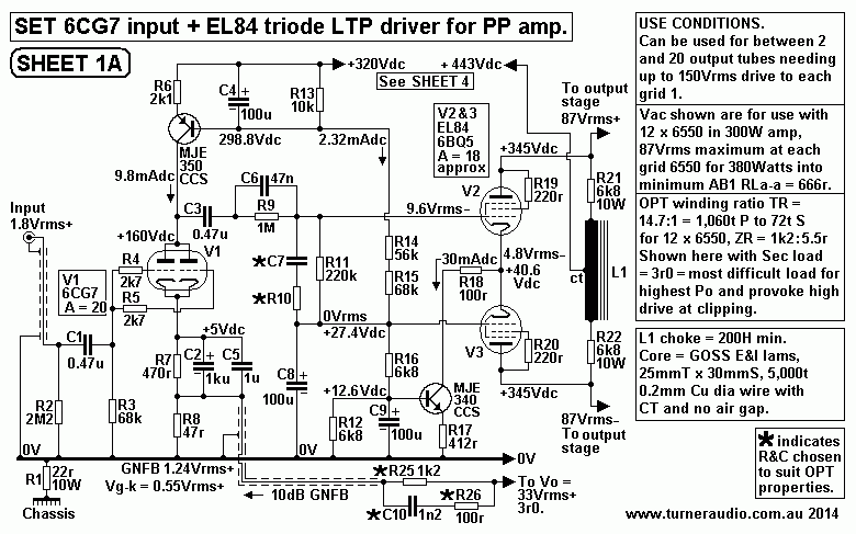
The triodes do all the actual work on the signal amplitude.
The input tube distortion of input and driver stage is reduced
about 10dB compared to
using only resistances to deliver dc to the tube anodes. Such
resistances are usually
less ohms than the following cap coupled biasing R, so that RLa
for 6CG7 would be
less than 6Ra and for EL84 would be 3Ra, which diminishes the
gain and the amount
of internal NFB which exists in each and every triode. The
higher anode load ohms
increases voltage gain to near µ and reduces THD while the Ra of
the triode is
minimized because with CCS or choke the Ia can be increased and
tube placed
within best operation region where gm is fairly high and linear.
Where anyone might use an input tube with different gain, the
global NFB
network R25, R26, C10 may have to be changed to maintain the
same
amount of applied global NFB.
I
show a Zobel network of R10 & C7 used to load V1 anode to
reduce V1 gain
and phase shift above 20kHz. In my amps such a Zobel network was
not needed.
But if you are going to build this amp, then you probably will
have an OPT with
less HF bandwidth and you will need to carefully trim some
values of R&C to give
unconditional LF and HF stability and give full Po bandwidth
20Hz to 65kHz
with rated load resistance and with 10dB GNFB.
The effect of the 6k6 also acts to
allow useful gain at very low F below 10Hz
where there is a very low audio signal content in music, while
also avoiding the
phase shift caused by L shunting Ra, so the L&R act as a
gain shelving network
and stability with NFB is OK. At F above 10Hz the 500H choke
reactance
increases at 6dB/octave and becomes a very high reactance load.
500H has Z = 31.5k at 10Hz, 315k at 100Hz, and much more for
most of
the audio band until its self capacitance begins to reduce its
reactance.
The resistance in series with the choke prevent the choke's
capacitive
reactance causing phase shift at the anode because the 6k6 is
several times
the Ra of each EL84 in triode.
Therefore the choke plus the series R provide a very high ohm
loading at
each EL84 anode and therefore the voltage swing can be maximized
without
the distortion which would occur if the choke was not used.
Therefore the resistance load value for each EL84 is mainly the
capacitance
coupled bias resistors used for each output tube.
In my amp I have 6 x 120k ohm grid
bias resistors on each side of the the PP
output stage.
All the bias supply ends of the 120k resistors are bootstrapped
to the cathode
feedback winding through Cc, Sheet 2 below.
Thus the anode load experienced see by each EL84 of the the LTP
is approximately
40kohms,
low enough to ensure good ac balance but high enough to ensure
THD of the
driver LTP stage is about -10 dB lower than if the dc was
brought to the
EL84 anodes via resistors which would have to be approximately
15k, which are
is really too low to get low THD.
The Ra of each EL84 as used = 2.2k approx, so the load of 40k =
18 x Ra which
ensures very low THD.
In other versions of this LTP with
EL84 I have tried using R&C cathode biasing networks
for each EL84 and found this gives closer balance of dc current
to each EL84 with no
detriment to signal operation. Non bypassed Rk will cause the
effective Ra to be much
higher, lower the stage gain, demand twice the drive voltage
from V1, and reduce the
bandwidth thus reducing the sonic dynamics. In my circuit here
with cathode feedback
in the output stage, the output tube grid signals are twice the
levels of using the plain
ultralinear configured amps.
I have found the idle current
balance in EL84 remains constant without any cathode
biasing over many years because the EL84 are set up with a very
low amount of Ia
compared to when used in an output stage with Ia = 40mA.
But here they have Ia = 15mA, so the EL84 should have a long
life without problems.
At normal levels and because of the
global NFB the overall THD is quite negligible
because THD is about proportional to output voltage.
There some obviously acceptable
other tubes that could be used for V2 and V3.
EL86 are pentodes which will work as well as EL84. EL86 gain is
1/2 that of EL84,
and Ea should be +250V, not +300V, so R between anode s and
choke would be
increased for a given B+. EL86 triode Ra is only 1.4k, so there
is some betterment
of open loop bandwidth. Using EL86 would mean the V1 gain would
need to be doubled
to produce about 20Vrms to LTP as I show it in Sheet 1A above.
EL86 are not manufactured any
longer. 6V6 could also be used and gain is very
similar to EL86. But Ra of the 6V6 triode is twice that of EL84.
The best choice is EL84.
For better performance to get higher
Va to drive tubes like 845 in PP, a pair of EL34
is hard to beat.
Since 2006, instead of V1
operating as a single ended stage as shown, I have tried
using a pair of triodes in
an LTP with cathode CCS. This allows for balanced drive to
the same following LTP stage using EL84. The CCS used in the
EL84 cathode circuit
may be replaced with a fixed resistance, say 5k6 to a negative
supply rail, say -150Vdc.
The signal input is fed into one grid of the input LTP and
global NFB fed into the other
grid of the V1 LTP. I have tried this on several re-engineered
amplifiers, ARC VT100, and
Dynaco MkVI, and was rewarded with astounding music and
excellent technical measurements.
One 2013 project was reforming a pair of RCA amps seen at Reformed
RCA 30W amps
The
page further explains the use for cascaded LTP input-driver
amps, and the
reformed RCA schematic is fine for where output drive voltage is
fairly low for
all OP tubes including KT88 in triode.
The
dual LTP idea may be used for higher Vo to suit my 300W amp with
local CFB
in using tertiary windings at the OPT, and here is what you
might use......
Sheet
1B.
Sheet
1B has changes to Sheet 1A but I have kept changes simple as
possible. Experimenters may use either Sheet 1A or Sheet 1B
while
making only minor changes to B+ and B- rail supplies shown on
Sheet 4.
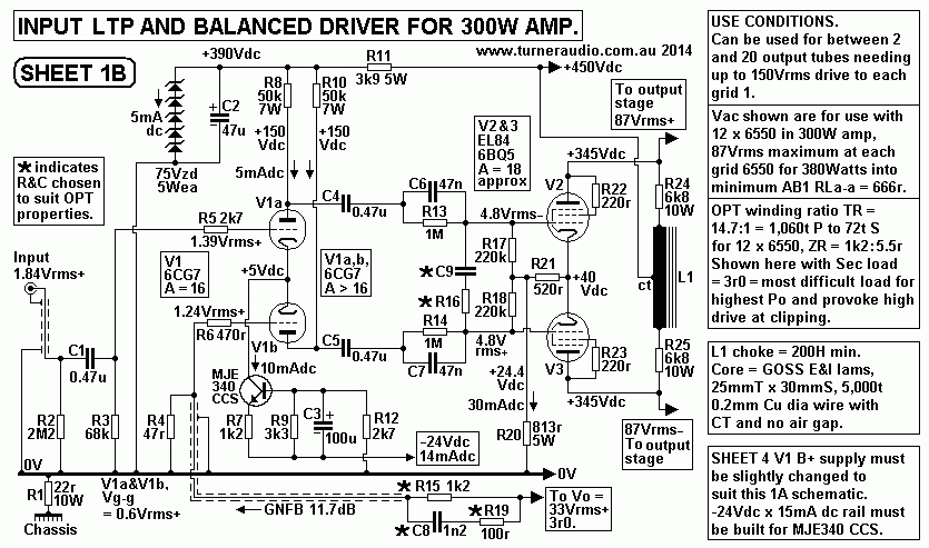
Sheet 1B does require a higher shunt regulated B+ rail for
V1a+b, and
the B- fixed bias supply must be changed to get an additional
-24Vdc
rail to provide for V1 current sink using MJE340. Sheet 4 has 2
diodes
used in a full wave rectifier off 12.6V-0-12.6V Vac heater
voltages producing
-17Vdc fixed bias for output tubes. The supply must be altered
so a doubler
rectifier to produce an additional -34Vdc rail which is RC
filtered down and
shunt regulated with 24V x 5W zener diode, so that 14mAdc is
available to
MJE340 and divider resistors.
The
6CG7 V1 input tube is used as an LTP with input ports to both
grids.
Input signal is to V1a grid and GNFB is to V1B grid. The
differential gain is
16x approx. THD of this differential pair or "LTP" is much less
than the Sheet 1A
version with SE V1a&b. Balance with 1% resistors will be
excellent and
each of V1a and V1b need only generate 4.8Vrms to feed V3 and V4
grids.
V3
and V4 are a balanced amp, with balanced output produced by a
balanced
input, giving least THD. The loading of anodes is the same as in
Sheet 1A and
includes the same CT choke L1. V3 and V4 can each produce
150Vrms before
clipping.
SHEET 2, OUTPUT STAGE FOR 300W AMPS.
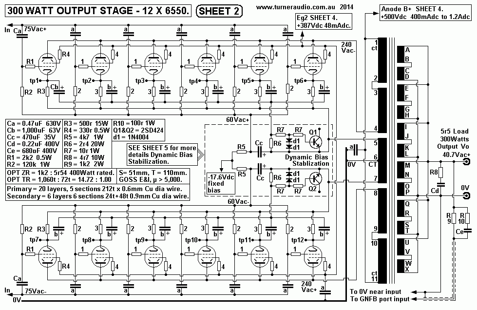
The Sheet 2 output stage
looks complex, but it is mostly repetition of a basic idea.
The R&C part identification seems strange but all resistors
and capacitors in similar
functions for each tube are just labelled with the same number
for R, and same letter
for C. I am sure any tech will get used to the idea which keeps
my schematic
uncluttered.
The
two balanced outputs from the V2 & V3 LTP driver amp anodes
on Sheet 1A
are fed to rails with 6 x 0.47u coupling caps Ca of 0.47 uF, on
each side of PP circuit.
R1 2k2 grid stoppers are used on each tube to prevent RF
oscillations.
Each output grid is biased with R2 120k, and all 6 on each side
of the PP circuit
are taken to a -17.6Vdc fixed bias supply via R5 4k7. Sheet 4
shows the bias
supply. The -17.6 fixed bias is bootstrapped by Cc 470uF to the
CFB windings on OPT.
This bootstrapping raises the effective ohm value of 6 parallel
120k R2 from 20k to
at least 43k. Thus the loading effect on V2&V3 of many bias
R2 is kept low.
Each output tube has separate R&C cathode biasing with R3 =
500r formed
with 3 x 1k5 each 5W. With B+ at +500V, and screen supply at
+387Vdc,
the Ek cathode bias voltage will be about +23Vdc, so idle Ea =
+477Vdc, and
Eg2 = +364Vdc. The 500r for R2 is high enough for good bias
regulation Ea
is kept usefully high and total idle grid bias -Eg1 = 23V +
17.6V = -40.6Vdc,
all without having a high amount of heat wasted in R2.
The
anode supply is about +500V with mains at 240Vac. Mains voltages
here change
between 235Vac at high mains load to 252Vac with low mains
loads. This means
B+ will vary between +489V to +525V which will not trouble the
6550 with possible
high Pda which at idle with Ea at 477V should be 19.1Watts. The
Eg2 is regulated
so Pdg2 is 4mA x 364V = 1.5W. Total Pda+Pdg2 = 20.6W which is
less than 1/2
of the max rating for 6550 of 42W.
At no time did I find that the tubes wanted to oscillate at
frequency well above
the audio band but it can happen when tubes become seriously
overheated.
R4 330 ohm screen stoppers are rated for only 1/4 W and will
burn open if Ig2
exceeds about 35mA. But if any one or more 6550 tubes overheat
the Ia and Ig2
flow in R3 500r R3 will increase thus raising Ek which triggers
active protection
turn off the power supply in Sheet 3 well before tubes could
seriously overheat.
On
each side of PP circuit the earthy ends of six R3 are taken to
one end of
the cathode FB winding on OPT.
Dynamic
Bias Stabilization is used.
The earthy ends of the six Cb caps, 1,000uF, are all taken to
top of R56 which are
2 x 4r7 10W. The R6 is a negligible ohm resistance but enough to
sense Ik flow
to CFB winding. During class A operation the Iac in R6 varies a
maximum of +/- 0.24A.
This produces Vac across R6 = +/-0.56V.
But during class AB operation the +Iac rise could be up to
2.3Amp. We might expect
to see V6 Vac rising to 5.4Vpeak. The top of R6 is connected to
Q1 base via
two R7 each 10r0. To prevent excessive base current input there
are two d1 diodes
to limit rise of Vce. The Q1 ( and Q2 ) base is being driven by
low resistance, needed
because Hfe of the Q1 is not high and base input resistance is
lowish.
As soon as class AB action commences and R5 positive voltage
peaks rise above
0.57V the bases turn on collector current which drains current
from Cb 1,000uF to
prevent them charging up . The Q1 and Q2 act to keep Ek steady
but only due to
signal effects. Meanwhile the Ek resulting from steady Ik is
allowed to remain
free to move. So all 6550 will have slightly different Ek. The
test points tp1 to tp12
are accessible through holes in side of chassis so that Ek for
each 6550 can be
checked with a voltmeter every 3 months. Should any 6550 develop
a fault so that
excessive Ia flows, then the amp automatically is turned off
internally, and my other
schematic sheets on active protection shows how this is done.
The Ikdc flow of the
6550 does not interfere with the action of Q1 or Q2 which only
act due to class AB
signal currents. These amps will spend most of their life acting
in pure class A so
the protection has little to do.
If Q1 and Q2 were not used, Ek rise with class AB could be from
+23Vdc to +63Vdc.
Such a rise would cause very serious audible distortions well
before clipping.
The
active bias stabilization gives the benefits of fixed bias but
also allows the
benefits of cathode "auto biasing" which eliminates the need of
a bias adjust pot
for each 6550. With 2 channels there are 24 x 6550, and 24
adjustments are far
too many to worry about.
Not
all the possible HF bandwidth is used when global NFB is added,
and bandwidth
is reduced with GNFB to 65kHz for stability reasons.
Load
match strappings of OPT are ideally for 2r5 or 5r6.
The 2r5 strapping suits speakers between 1r3 to 5r0.
The 5r6 strapping suits anything over 3r5.
The
nominal anode load is 1k2 for 12 x 6550, so the loading is easy
and each pair
of 6550 in the output stage has a load of 7k2 for a high amount
of initial class A.
The Class A power is 34Watts before AB power begins. An absolute
maximum
power of 450W with sine wave drive is possible.
It
is a somewhat complicated task for a non technical person to
change output
transformer matching, so the default setting is the 5.6 ohm load
match.
Some speakers have appalling impedance curves with dips in Z
well below their
nominal claimed Z but this amp design will handle them all with
ease.
The
only stabilizing zobel network needed is the 4.7 ohms + 0.22uF
across the output
terminals. Thus at 154kHz, the reactance Ce 0.22uF = R7 4r7 so
as frequency rises
above 160kHz there is an increasingly resistive load across the
output terminals.
Any
value of capacitance across the output terminals and without any
parallel or
series resistance load does not provoke any HF oscillations.
Picture
of 300W amp under-chassis with nearly completed work.
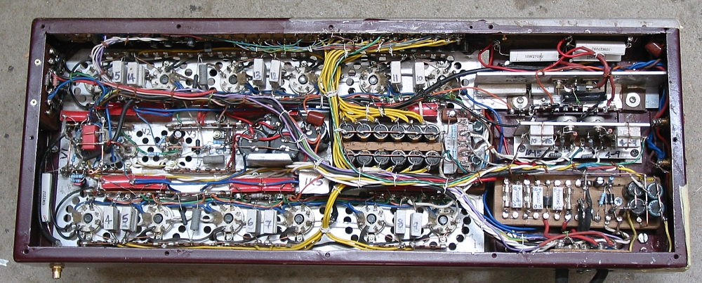
You
are at 300W
amp input/driver and output stages
Other
pages on 300W amps.....
300W amp power supply
300W amp active protection
300W amp dynamic bias
stabilization
300W amp power vs load
graphs
300W amp images, tubes with blue
glow, and more views of amps
Back to Power amplifiers
Back to Index Page